Microoptical compound lens

a compound lens and microoptic technology, applied in the field of microoptics, can solve the problems of reducing the resolution and image quality of microoptical lenses, diffraction-limited performance to be achieved, and optic limitations due to geometric aberrations to be overcome, so as to improve the overall fov, improve the numerical aperture, and improve the effect of image quality

Inactive Publication Date: 2007-10-23
SANDIA
View PDF11 Cites 72 Cited by
  • Summary
  • Abstract
  • Description
  • Claims
  • Application Information

AI Technical Summary

Benefits of technology

[0011]The hollow optical shell can be a transparent glass or plastic hemispherical shell. The lenslets can comprise aspherical and/or diffractive surfaces for improved image quality. The spacing shell can comprise an absorbing material with a plurality of holes cut therethrough along the optical axes of the lenslet pairs to remove stray incoming rays and prevent crosstalk between the optical paths of adjacent lenslet pairs. The coherent fiber bundle can comprise a plurality of single-mode optical fibers that are straight and parallel to the centerline of the b...

Problems solved by technology

However, diffraction effects can drastically reduce the resolution and image quality of a microoptical lens.
Further, optic limitations due to geometric aberrations must be overcome for diffraction-limited performance to be achieved.
Whereas these aberrations can be mitigated in conventional lens systems using a train of multiple refractive lenses having weakly curved surfaces or lenses having aspheric surfaces, correcting aberrations becomes a major problem with microoptical systems.
This is because packaging and alignment of multiple microoptical elements in a train is very difficult and fabricating aspheric microoptical surfaces is challenging.
However, single-aperture eyes are very massive and energy-consumptive for small creatures.
Whereas the resolution of a compound eye is usually poor compared to the single-aperture eye, the poorer resolution is counterbalanced by ...

Method used


Image

  • Microoptical compound lens
  • Microoptical compound lens
  • Microoptical compound lens

Examples


Embodiment Construction

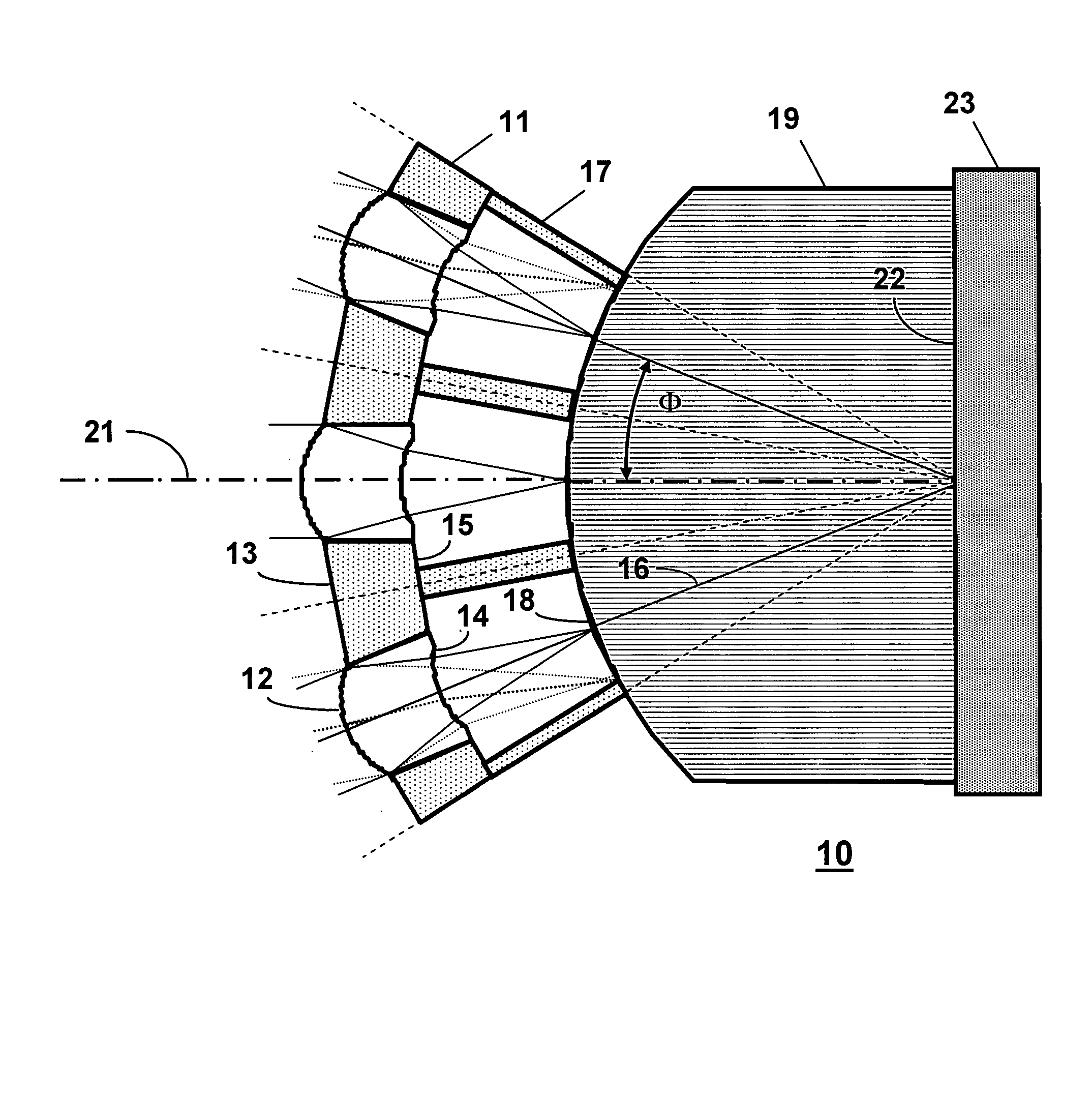
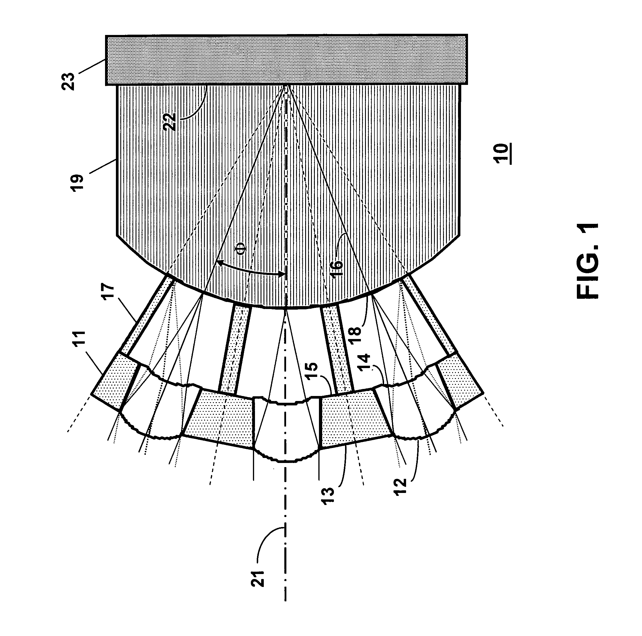
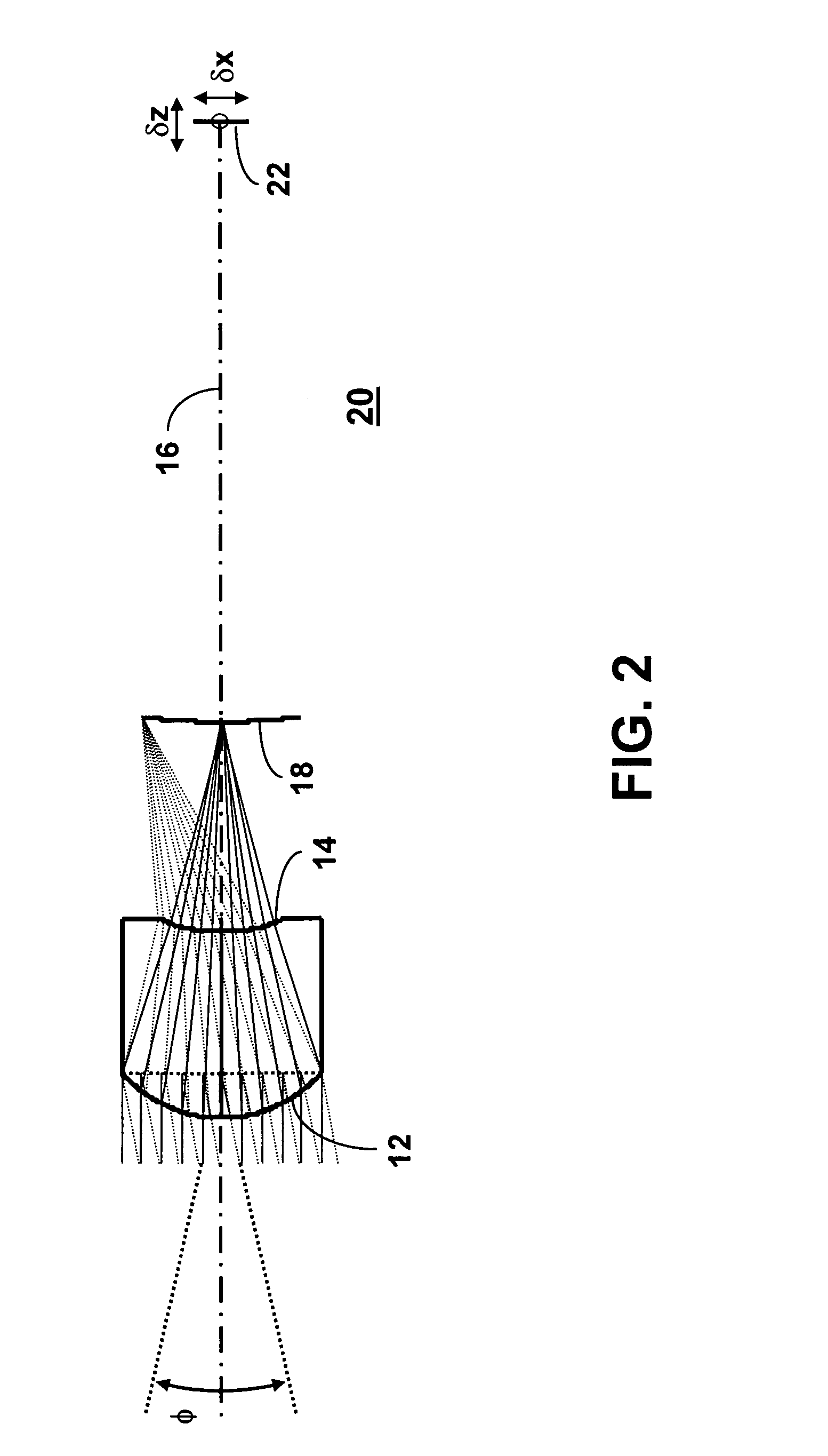
[0016]In FIG. 1 is shown an example of an apposition microoptical compound lens 10 having a plurality of artificial ommatidia for imaging light from an object. The lens 10 comprises a segment of a hollow, three-dimensional optical shell 11 with an array of lenslets formed on the inner and / or outer surfaces of the shell. Outer lenslets 12 on the outer shell surface 13 collect light from the object. The outer lenslets 12 can be precisely aligned on an ommatidial axis 16 with corresponding inner lenslets 14 on the inner shell surface 15. Each lenslet pair 12 and 14 is aligned on a separate ommatidial optical axis 16. The angle between the optical axes of two adjacent lenslet pairs is known as the interommatidial angle Φ. The optical rays from each lenslet pair 12 and 14 are focused and create a sub-image on the curved front surface 18 of a coherent fiber bundle 19. The curved front surface 18 of the coherent fiber bundle 19 is concentric with the hollow optical shell 11. A curved space...


PUM


Abstract

An apposition microoptical compound lens comprises a plurality of lenslets arrayed around a segment of a hollow, three-dimensional optical shell. The lenslets collect light from an object and focus the light rays onto the concentric, curved front surface of a coherent fiber bundle. The fiber bundle transports the light rays to a planar detector, forming a plurality of sub-images that can be reconstructed as a full image. The microoptical compound lens can have a small size (millimeters), wide field of view (up to 180°), and adequate resolution for object recognition and tracking.

Description

STATEMENT OF GOVERNMENT INTEREST[0001]This invention was made with Government support under contract no. DE-AC04-94AL85000 awarded by the U.S. Department of Energy to Sandia Corporation. The Government has certain rights in the invention.FIELD OF THE INVENTION[0002]The present invention relates to microoptics and, in particular, to an microoptical compound lens for imaging an object.BACKGROUND OF THE INVENTION[0003]The growth of the microelectronic, microelectromechanical systems (MEMS), and optical fiber telecommunication industries has driven a need for microoptical systems. In particular, the miniaturization of security and defense systems has created a need for high precision micro- and meso-scale optical systems for miniature robotic navigation and vision systems, surety devices, verification sensors, handheld imaging systems, and portable chemical and biological detection systems. The compactness of microoptical systems offers the advantages of portability and increased functi...

Claims


Application Information

Patent Timeline
IPC IPC(8): G02B27/10
CPCG02B3/0037G02B3/08G02B6/4206G02B3/0056
Inventor SWEATT, WILLIAM C.GILL, DAVID D.
Owner SANDIA
Why Eureka
Try Eureka