Semiconductor equipment

a technology of semiconductor equipment and equipment, applied in the direction of generating/distributing signals, pulse techniques, instruments, etc., can solve the problems of electromagnetic interference and electromagnetic interference, and achieve the effect of easy to achieve semiconductor equipmen

Active Publication Date: 2007-10-30
PANASONIC SEMICON SOLUTIONS CO LTD
View PDF6 Cites 3 Cited by
  • Summary
  • Abstract
  • Description
  • Claims
  • Application Information

AI Technical Summary

Benefits of technology

[0008]In the present invention, a source clock is inputted to a delay circuit, a counter circuit is operated in response to a delay clock which is the output of the delay circuit, and a clock used as a system clock is selected from the source clock and the delay clock based on the value of the counter circuit. With this configuration, it is possible to easily change the duty cycle of the system clock, thereby achieving semiconductor equipment hardly causing electromagnetic interference.
[0009]Semiconductor equipment according to the first aspect of the present invention comprises an oscillator circuit which is connected to an oscillator or a radiator and outputs a source clock, an internal circuit operating in synchronization with a system clock, a delay circuit for generating a delay clock delayed by a specified time from the source clock outputted from the oscillator circuit, a counter circuit for counting the delay clock, and a selector circuit which selects the source clock and the delay clock based on the value of the counter circuit and outputs the system clock to the internal circuit. With this configuration, the clock is selected in response to a selection signal controlled by the delay clock, so that it is possible to obtain semiconductor equipment which can simplify timing control, can readily change the duty cycle of the system clock, and hardly causes electromagnetic interference.
[0010]According to the second aspect of the present invention, the semiconductor equipment according to the first aspect is characterized in that only the least significant bit has an initial value of “1” and other bits have initial values of “0” in the counter circuit. With this configuration, the counter circuit can be shared with a timer circuit in the semiconductor equipment. It is possible to obtain semiconductor equipment which hardly causes electromagnetic interference while further suppressing an increase in circuit size.
[0012]Semiconductor equipment according to the fourth aspect of the present invention comprises an oscillator circuit which is connected to an oscillator or a radiator and outputs a source clock, an internal circuit operating in synchronization with a system clock, a first delay circuit for generating a first delay clock delayed by a specified time from the source clock outputted from the oscillator circuit, a second delay circuit for generating a second delay clock delayed from the first delay clockby the specified time, a delay clock selector circuit which selects and outputs the first delay clock or the second delay clock, a counter circuit for counting the second delay clock, and a selector circuit for selecting the source clock and the output clock of the delay clock selector circuit based on the value of the counter circuit and outputs the system clock to the internal circuit. With this configuration, by switching delay values, harmonic noise in a specific frequency band can be reduced, thereby obtaining semiconductor equipment hardly causing electromagnetic interference.
[0014]As described above, the present invention makes it possible to easily achieve a semiconductor equipment which hardly causes electromagnetic interference with a simple circuit configuration.

Problems solved by technology

As a result, harmonic current passes through the internal circuit and flows to the outside, resulting in electromagnetic interference and so on (Japanese Patent Laid-Open No. 5-152908).
Under present circumstances, in semiconductor equipment where internal elements repeat high-speed switching in synchronization of a system clock, high-order harmonics are generated and result in electromagnetic interference.

Method used


Image

  • Semiconductor equipment
  • Semiconductor equipment
  • Semiconductor equipment

Examples


embodiment 1

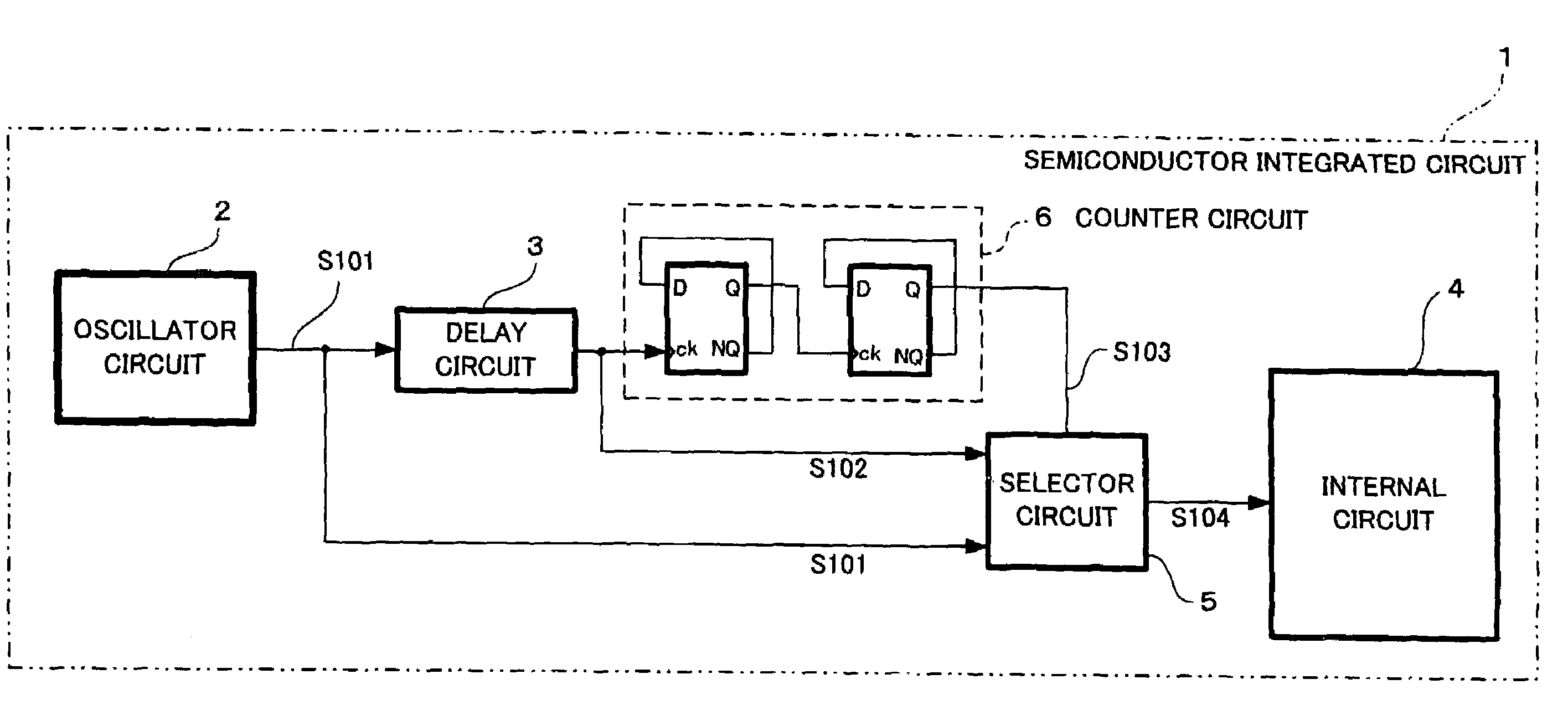
[0028]FIGS. 1 to 4 show (Embodiment 1) of the present invention.

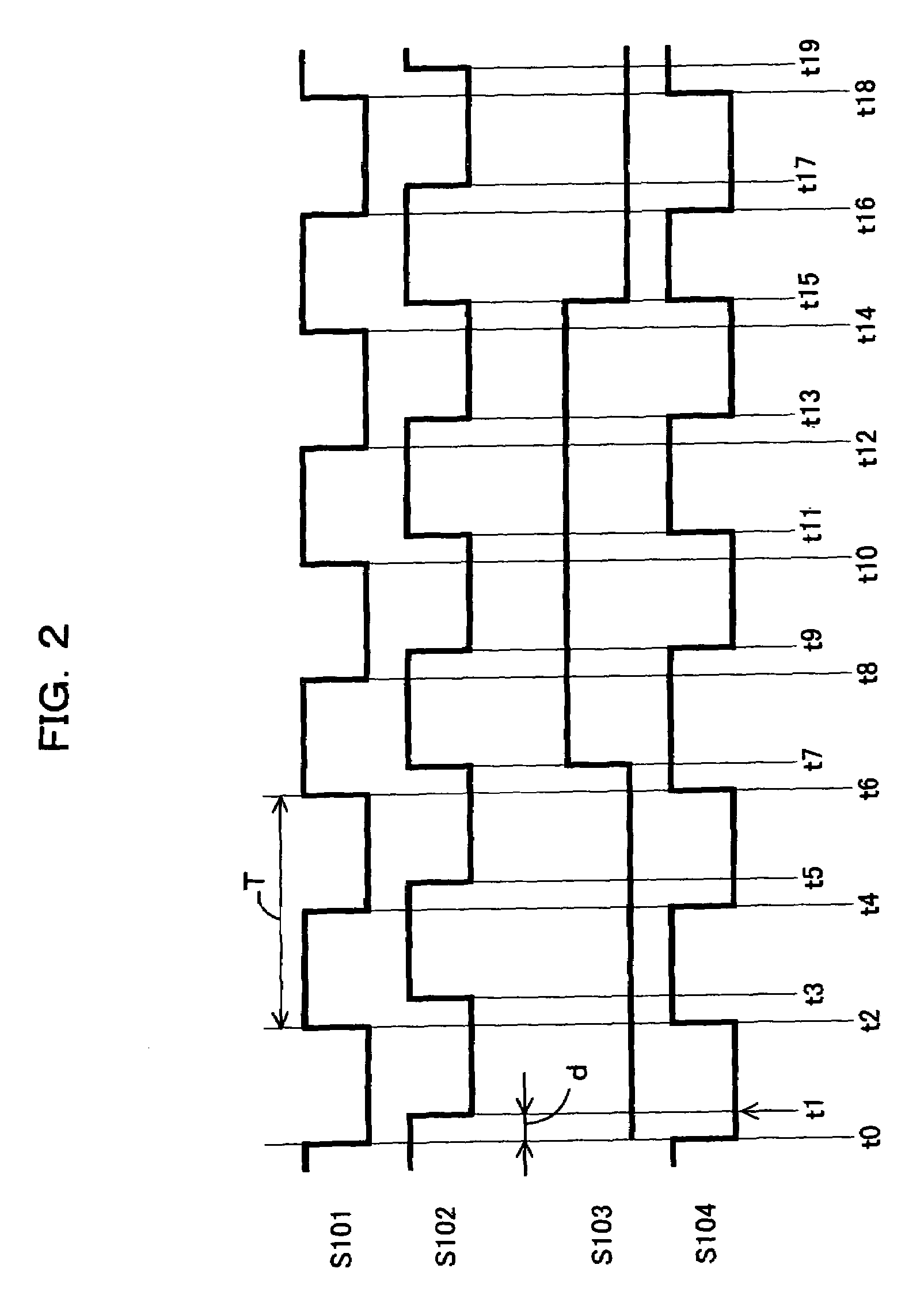
[0029]FIG. 1 shows semiconductor equipment of the present invention. FIG. 2 is a signal waveform chart of the semiconductor equipment. FIGS. 3 and 4 are current spectrum diagrams.

[0030]In semiconductor equipment 1 having an internal circuit 4 operating in synchronization with a system clock, a logic circuit constituted of a delay circuit 3, a counter circuit 6, and a selector circuit 5 is interposed between the clock input of the internal circuit 4 and an oscillator circuit 2 which is connected to an oscillator or a radiator and outputs a source clock S101. The source clock S101 has a frequency of f0 and a period of T.

[0031]The delay circuit 3 outputs a delay clock S102 which is obtained by delaying the source clock S101 from the oscillator circuit 2 by a specified time d.

[0032]The counter circuit 6 is a 2-stage counter circuit for counting the delay clock S102 outputted from the delay circuit 3. As shown in FIG. 2, an ...

embodiment 2

[0047]FIG. 5 shows (Embodiment 2) of the present invention.

[0048]FIG. 5 shows another example of the counter circuit 6 shown in FIG. 1. An oscillator circuit 2, a delay circuit 3, a selector circuit 5, and an internal circuit 4 of semiconductor equipment of (Embodiment 2) are similar to those of (Embodiment 1).

[0049]In FIG. 5, a counter circuit 6 is characterized in that only the least significant bit has an initial value of “1” and other bits have initial values of “0” in response to an initializing signal S129.

[0050]A flip-flop 29 is fed with an overflow signal outputted from the counter circuit 6 and uses a system clock S104 as a clock.

[0051]The following will discuss the operations of the semiconductor equipment configured thus according to (Embodiment 2).

[0052]A source clock S101 with a frequency of f0 and a period T generates a delay clock S102 delayed by a specified time by the delay circuit 3. In response to an output signal S123 of the counter circuit 6, the selector circui...

embodiment 3

[0058]FIGS. 6 and 8 show (Embodiment 3) of the present invention.

[0059]FIG. 6 shows another example of the delay circuit 3 shown in FIG. 1. An oscillator circuit 2, a counter circuit 6, a selector circuit 5, and an internal circuit 4 of semiconductor equipment of (Embodiment 3) are similar to those of (Embodiment 1). FIG. 8 is a signal waveform diagram.

[0060]Reference numerals 33a and 33b denote first and second delay circuits. A source clock S101 is inputted to the first delay circuit 33a where a delay value is a specified time d1. A delay clock S132a generated on the output of the first delay circuit 33a is outputted as a delay clock S132b through the second delay circuit 33b where a delay value is a specified time d2.

[0061]Reference numeral 34 denotes a delay clock selector circuit. The delay clocks S132a and S132b are inputted to the input of the delay clock selector circuit 34. One of the delay clocks S132a and S132b is selected in response to a selection signal S136 and is out...


PUM


Abstract

There is provided a semiconductor integrated circuit in which a source clock (S101) is inputted to a delay circuit (3), a counter circuit (6) is operated in response to a delay clock (S102) which is the output of the delay circuit (3), a clock used as a system clock by an internal circuit (4) is selected from the source clock (S101) and the delay clock (S102) based on the value of the counter circuit (6), and the duty cycle of the system clock is changed, so that it is possible to reduce electromagnetic interference resulting from harmonics generated by the switching of the internal circuit.

Description

FIELD OF THE INVENTION[0001]The present invention relates to semiconductor equipment comprising an internal circuit operating in synchronization with a system clock signal.BACKGROUND OF THE INVENTION[0002]In an internal circuit of conventional semiconductor equipment, internal elements repeat high-speed switching in synchronization with a signal called a system clock. As a result, harmonic current passes through the internal circuit and flows to the outside, resulting in electromagnetic interference and so on (Japanese Patent Laid-Open No. 5-152908).[0003]FIG. 10 shows such conventional semiconductor equipment.[0004]A semiconductor chip 101 serving as semiconductor equipment comprises an oscillator circuit 2 to which an oscillator or a radiator is connected and an internal circuit 4 which operates in synchronization with a system clock S191 outputted from the oscillator circuit 2. FIG. 11 shows the system clock S191 and the current waveform of the internal circuit 4 of the semicondu...

Claims


Application Information

Patent Timeline
Patent Type & Authority Patents(United States)
IPC IPC(8): G06F1/04G06F1/08
CPCG06F1/04
Inventor YONEDA, TAKASHI
Owner PANASONIC SEMICON SOLUTIONS CO LTD
Why Eureka
Try Eureka