Method and apparatus for semiconductor device and semiconductor memory device

a semiconductor memory and semiconductor technology, applied in semiconductor devices, electrical devices, instruments, etc., can solve the problems of inability to teach the effects of these two types of holes on the injection mechanism, the injection scheme employed in prior art is believed to suffer from the following problems, and the cell needs to be considered. to achieve the effect of suppressing the large c

Inactive Publication Date: 2007-11-20
MARVELL ASIA PTE LTD
View PDF78 Cites 11 Cited by
  • Summary
  • Abstract
  • Description
  • Claims
  • Application Information

AI Technical Summary

Problems solved by technology

However, there are several fundamental problems associated with the charge injection mechanism and energy band structure in the noted article.
Further, there are fundamental problems when such mechanism and band structure are employed for non-volatile memory operation.
Moreover, there are several problems in the prior art memory cell need to be considered.
Further, the prior art did not teach the effects associated with these two types of holes on the injection mechanism.
Thus, the injection scheme employed in prior art is believed to suffer from following problems:
Thus, a ballistic HH is more prone to loose its ballistic nature during its transport in a semiconductor region.
In other words, when ballistic holes are employed for erasing prior art memory cells, since the majority population of the hole carriers are of the HH type, which has a shorter mean-free-path, most of the supplied holes cannot contribute to the erase operation as anticipate.
This causes waste on total current.
The aforementioned effects were ignored in prior art memory cells, and hence the cells require more electrical current be supplied, thus consuming more electric power, in order to complete an erase operation.
Further, the low hole injection efficiency in prior art cells can result in slow erase problem when implementing the cells in their product applications.
In other words, the current of backward injected electrons in prior art cell cannot be-entirely suppressed.
Further, there are several other fundamental deficiencies on the symmetrical tunneling structure and cell structure of prior art.
Therefore it cannot function properly.
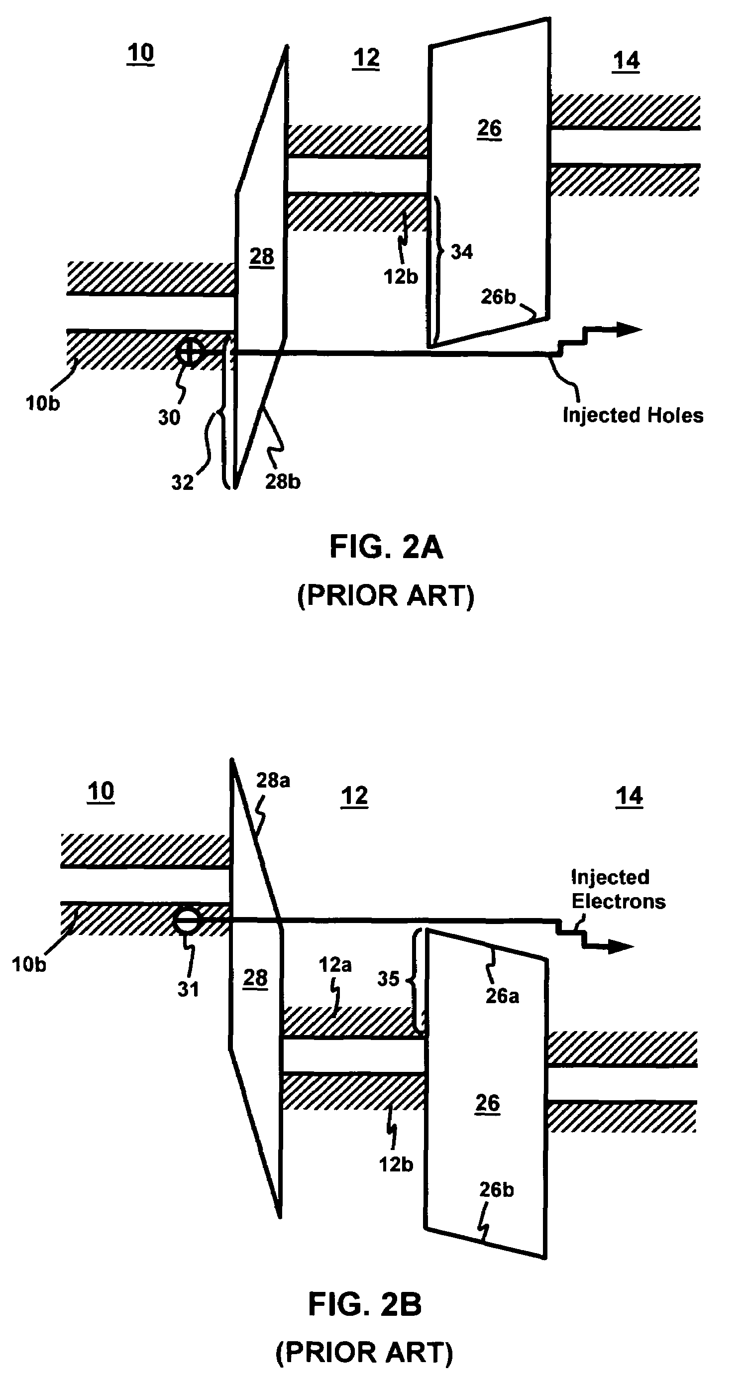
Parasitic holes backward injection problem is another major problem for the mechanism employed in prior art.
The problem on backward injected holes 38 is caused by the requirement on higher work function in prior art.
Therefore, the symmetrical tunneling structure of prior art cannot be optimized to suppress parasitic charge carriers for both program and erase operations simultaneously.
This requirement results in larger cell size, and limits the cell of prior art from practical application.
This problem also exists in operating the amplifier by Mead, wherein metal is employed as the material for base, which is equivalent to the ballistic gate 12 in FIG. 3B.
The backward injected holes can unduly increase the base current of the amplifier, and hence degrade the performance of such device when used an amplifier.
In addition to the problems described above, the injection mechanism and energy band structure employed in prior art also can suffered from impact ionization problem. FIG. 3B shows the impact ionization problem in the prior art band structure in FIG. 2B.
The holes 40a are highly energized and can be backward injected to gate 10 creating traps in dielectric 28 as passing through, thus causing reliability problem.
These effects are uncontrollable, where current can unduly increase to result in current loading issue on supporting circuitry for memory operations.
The effects further cause reliability problem.
The cell structure in prior art thus demands stringent control on the threshold voltage, and is believed having low manufacturability yield and difficulties in practical applications.
The backward injected electrons 37 have energy high enough to impact ionize charge carriers in tunneling gate 10 to cause loading issue on supporting circuitry and reliability problem.
The injection mechanism, energy band and cell structure in prior art thus face similar issues in both the program and the erase operations, and the memory is believed having low manufacturability yield and difficulties in practical applications.
The cell structure in prior art thus demands stringent control on the dielectric breakdown, and is believed having difficulties in practical applications.
Therefore, it results in a large parasitic capacitance C between gates 10 and 12, and is undesirable as it introduces adverse impact on cell operation.
Therefore, the cell architecture in prior art further suffer from the compromise between suppressing the parasitic electrons and suppressing the total capacitance of ballistic gate 12.
The needs on a thin thickness unavoidably results in a high sheet resistance to that layer.
Therefore, prior art suffers from a much larger resistance R on both tunneling gate 10 and ballistic gate 12.
First, it can cause a large signal delay due to the combining effects of the large R and the large C (i.e. the RC delay).
This is particularly a main issue on cell operation as the RC delay can limit the speed on accessing a memory cell when embedded in a large memory array.
However, due to the RC delay, voltages on un-selected cells can be different than the desired values, and hence cell disturb is more prone to happen.
Furthermore, the large R can combine with a large current I to result in a IR effect, which can cause a voltage drop when passing a voltage in a signal line.
The effect prevents the voltage on a designated electrode of a memory cell from reaching its desired level, and hence can adversely impact cell operation.
This results in weak voltage-dependence on the current-voltage relationship.
Therefore, unselected cells in prior art are prone to cell disturb issues in both program and erase operations.
Further, another major problem encountered by the transistor is to do with the low transfer ratio due to the low efficiency of the injection mechanism.
However, the efficiency typically still ranges from about 0.01 to about 0.4, and thus prevents the transistor from practical applications.

Method used


Image

  • Method and apparatus for semiconductor device and semiconductor memory device
  • Method and apparatus for semiconductor device and semiconductor memory device
  • Method and apparatus for semiconductor device and semiconductor memory device

Examples


Embodiment Construction

[0085]Embodiments of the present invention described in the following detailed description are directed at injection mechanisms, methods and memory cell structures. Those of ordinary skill in the art will realize that the detailed description is illustrative only and is not intended to restrict the scope of the claimed inventions in any way. Other embodiments of the present invention, beyond those embodiments described in the detailed descriptions, will readily suggest themselves to those of ordinary skill in the art having the benefit of this disclosure. Reference will now be made in detail to implementations of the present invention as illustrated in the accompanying drawings. Where appropriate, the same reference indicators will be used throughout the drawings and the following detailed description to refer to the same or similar parts.

[0086]In the interest of clarity, not all of the routine features of the implementations described herein are shown and described. It will be appr...


PUM


Abstract

Method and apparatus on charges injection using piezo-ballistic-charges injection mechanism are provided for semiconductor device and nonvolatile memory device. The device comprises a strain source, an injection filter, a first conductive region, a second conductive region, and a charge collecting region. The strain source permits piezo-effect in ballistic charges transport to enable the piezo-ballistic-charges injection mechanism in device operations. The injection filter permits transporting of charge carriers of one polarity type from the first conductive region, through the filter, and through the second conductive region to the charge collecting region while blocking the transport of charge carriers of an opposite polarity from the second conductive region to the first conductive region. The present invention further provides an energy band engineering method permitting the devices be operated without suffering from disturbs, from dielectric breakdown, from impact ionization, and from undesirable RC effects.

Description

RELATED APPLICATIONS[0001]This application claims the benefit of U.S. Provisional Patent Application Ser. No. 60 / 585,238 filed Jul. 1, 2004 and U.S. Provisional Patent Application Ser. No. 60 / 626,326 filed Nov. 8, 2004. This application is a Continuation-In-Part of U.S. patent application Ser. No. 11 / 007,907 filed on Dec. 8, 2004, now U.S. Pat. No. 7,115,942 entitled “METHOD AND APPARATUS FOR NONVOLATILE MEMORY”. This application is also a Continuation-In-Part of U.S. patent application Ser. No. 10 / 457,249 filed on Jun. 6, 2003, U.S. Pat. No. 6,958,513 entitled “FLOATING-GATE MEMORY CELL HAVING TRENCH STRUCTURE WITH BALLASTIC-CHARGE INJECTOR AND ARRAY OF MEMORY CELLS”.TECHNICAL FIELD[0002]The present invention relates to semiconductor device and semiconductor memory device. More particularly, the present invention relates to methods and apparatus on transporting charges in these devices using piezo-ballistic-charges injection mechanism. Charge states of memory devices can be altered...

Claims


Application Information

Patent Timeline
Patent Type & Authority Patents(United States)
IPC IPC(8): H01L21/311H01L21/8247H01L27/115H01L29/423H01L29/788
CPCH01L27/115H01L27/11521H01L27/11568H01L29/792H01L29/42336H01L29/7881H01L29/7883H01L29/7885H01L29/42324G11C16/0416H10B69/00H10B41/30H10B43/30
Inventor WANG, CHIH-HSIN
Owner MARVELL ASIA PTE LTD
Why Eureka
Try Eureka