
Test apparatus and test method

a test apparatus and test method technology, applied in the field of test apparatus and test method, can solve the problems of difficult control of the gradient of the rising of the power supply voltage possible defects, and possible failures of the test apparatus, so as to reduce the gate voltage and increase the power supply voltage

Active Publication Date: 2007-11-20
ADVANTEST CORP
View PDF2 Cites 12 Cited by
  • Summary
  • Abstract
  • Description
  • Claims
  • Application Information

AI Technical Summary

Benefits of technology

The present invention provides a test apparatus and method for testing a device under test. The test apparatus includes a reference voltage supply section, a field effect transistor, and an inductance. The field effect transistor is connected between the reference voltage supply section and the device under test. The control section controls the gate voltage of the field effect transistor to change the power supply voltage to the device under test. The judgment section uses the power supply current value to determine the quality of the device under test. The test method involves controlling the gate voltage and judging the quality of the device under test based on the change in power supply voltage. The technical effect of the invention is to provide a more efficient and accurate method for testing devices.

Problems solved by technology

Since insulating portions of high withstand voltage semiconductor devices contain capacitance, a defect may possibly occur attributable to a size of the gradient of the rising of a power supply voltage for example.
In view of this, chances are that a defect may be detected when the gradient of the rising of the power supply voltage is larger than a predetermined value, while a defect may not be detected when the gradient is the predetermined value or smaller.
However, when testing a high withstand voltage semiconductor device, it is hard for a test apparatus to control the gradient of the rising of a power supply voltage to be supplied because the power supply voltage to be supplied is high.

Method used


Image

  • Test apparatus and test method
  • Test apparatus and test method
  • Test apparatus and test method

Examples


Embodiment Construction

[0019]As follows, the present invention is described based on some embodiments that do not intend to limit the scope of the present invention. All of the features and combinations thereof disclosed in the following are not necessarily essential to means provided by the aspects of the invention.

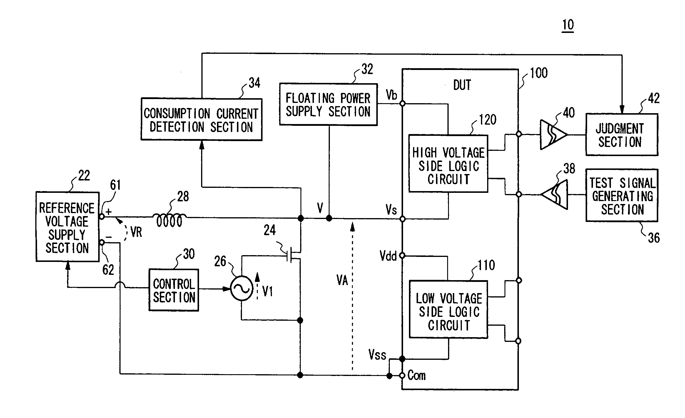
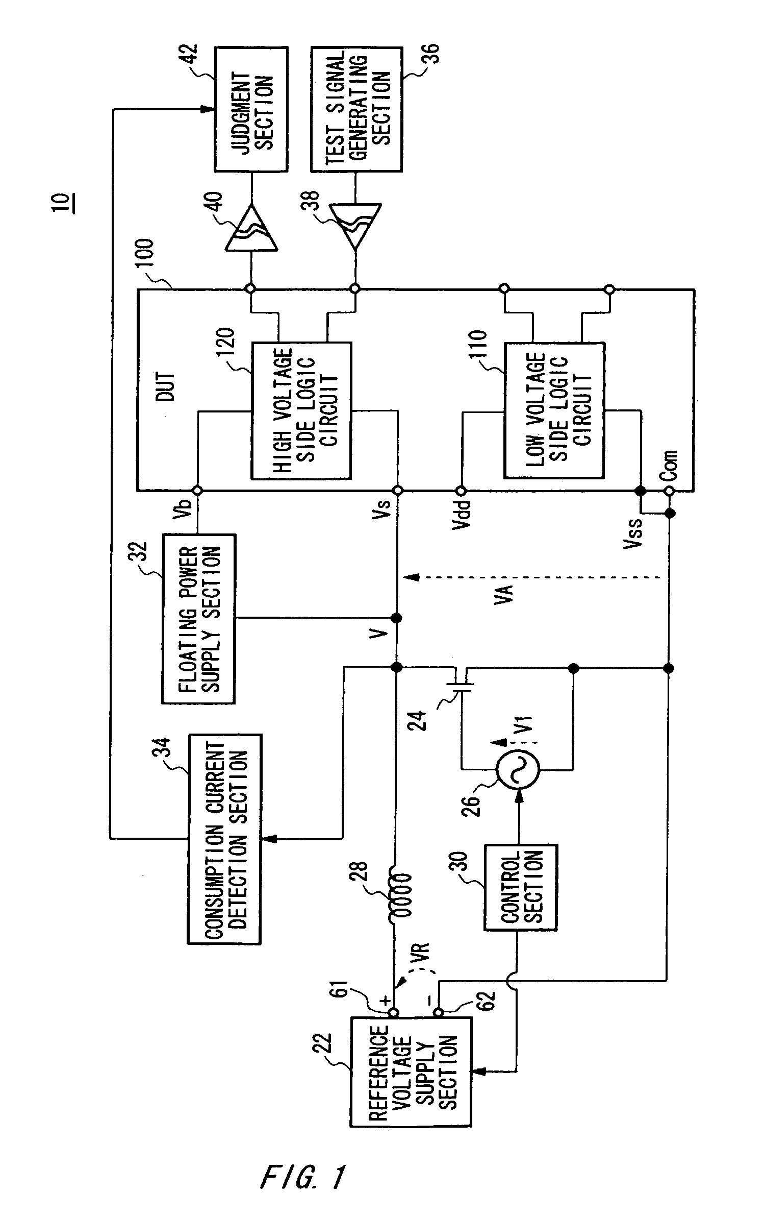
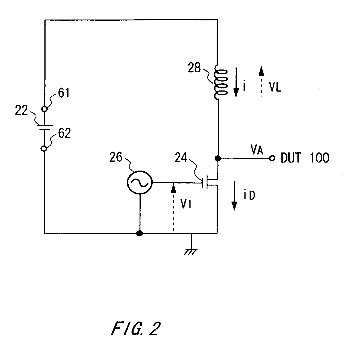
[0020]FIG. 1 shows a test apparatus 10 according to the present embodiment, together with a device under test (hereinafter referred to as “DUT 100”). The DUT 100 may include a low voltage side logic circuit 110 and a high voltage side logic circuit 120, for example. The low voltage side logic circuit 110 and the high voltage side logic circuit 120 are insulated from each other, and are operated with different potentials as references respectively. For example, when the low voltage side logic circuit 110 is operated with 0V as a reference, the high voltage side logic circuit 120 may be operated with from some ten volts to some kilovolts as a reference. It should be noted that the reference pote...


PUM


Abstract

Change in power supply voltage supplied to a device under test is controlled. There is provided a test apparatus for testing a device under test, the test apparatus including: a reference voltage supply section for supplying a reference voltage; a field effect transistor provided between a positive side terminal and a negative side terminal of the reference voltage supply section, so that a drain terminal and a source terminal of the field effect transistor are in parallel connection with the device under test; an inductance that is connected between the positive side terminal and the negative side terminal of the reference voltage supply section, the inductance being in serial connection with the device under test between a positive-side power supply terminal and a negative-side power supply terminal of the device under test, and being in serial connection with the field effect transistor between the drain terminal and the source terminal of the field effect transistor; a control section for controlling a gate voltage of the field effect transistor, thereby changing a power supply voltage to be supplied to the device under test; and a judgment section for judging quality of the device under test, based on characteristic of the device under test in accordance with change in the power supply voltage.

Description

CROSS REFERENCE TO RELATED APPLICATION[0001]The present application claims priority from a Japanese Patent Application No. 2006-025987 filed on Feb. 2, 2006, the contents of which are incorporated herein by reference.BACKGROUND[0002]1. Technical Field[0003]The present invention relates to a test apparatus and a test method. In particular, the present invention relates to a test apparatus and a test method for testing characteristic of a device under test by changing a power supply voltage.[0004]2. Related Art[0005]Semiconductor devices having high withstand voltage (hereinafter high withstand voltage semiconductor devices) are known to be used for controlling motors of electric cars and for controlling alternate current fan motors, for example. In such a high withstand voltage semiconductor device, PN conjunction is separated by means of an insulating film of SiO2 for example, and so it is possible to incorporate circuits operating under low voltages and circuits operating under hig...

Claims


Application Information

Patent Timeline
Patent Type & Authority Patents(United States)
IPC IPC(8): G01R31/08G01R31/02G01R31/26
CPCG01R31/1263
Inventor AMANUMA, SEIJI
Owner ADVANTEST CORP
Learn More