Digital clock switching means

a technology of digital clock and switching means, which is applied in the direction of generating/distributing signals, pulse characteristics measurement, pulse technique, etc., can solve the problems of wasting energy in generating another clock on the chip, no external clock may be available, and high cost of producing many different variants of an integrated circui

Active Publication Date: 2007-11-20
INFINEON TECH AG
View PDF7 Cites 21 Cited by
  • Summary
  • Abstract
  • Description
  • Claims
  • Application Information

AI Technical Summary

Benefits of technology

[0013]In one embodiment, each finite state machine comprises a counter with a variable (Cnt1; Cnt2), wherein the counter associated with the active clock source will get its variable (Cnt1; Cnt2) initialized to a constant (Nfail1, Nfail2) when said input signal (Select) indicates the switching off of the active clock source, whereby the finite state machine associated with the active clock source enters a CHECK state, and wherein the respective counter decrements the variable (Cnt1; Cnt2) at each clock cycle. If the other finite state machine verifies the presence of its clock source before the variable (Cnt1; Cnt2) reaches zero, the switch of the active clock source will be effected. If, on the other hand, the variable (Cnt1; Cnt2) decrements to zero and no such verification has occurred, no switch of the active clock source will be effected. The main advantage with the digital clock switching circuit according to the invention is that it guarantees that the system never enters a deadlock state in the absence of one clock source.
[0015]Furthermore, it is an advantage in another embodiment if the clock enable signal (Clk_En1; Clk_En2) of each finite state machine is connected, via a first double latch synchronizer, to an input (Other ClkEn2; Other ClkEn1) of the other finite state machine, whereby each finite state machine is able to monitor the state of the other clock enable signal (ClkEn2, ClkEn1) via said input (Other ClkEn1, Other ClkEn2).
[0016]In still another embodiment, a further advantage is achieved if each finite state machine is connected to a second double latch synchronizer, whereby said input signal (Select) passes via said second double latch synchronizer.
[0017]In yet another embodiment, it is an advantage if the first clock source (Clk_A) is connected to and controls the first and second double latch synchronizers connected to the first finite state machine, and the second clock source (Clk_B) is connected to and controls the first and second double latch synchronizers connected to the second finite state machine.

Problems solved by technology

The motivation for such a design is flexibility and reduced power consumption: in some applications, there could already be an externally generated clock available and so to generate another clock on-chip is wasteful of energy.
In other applications, no such external clock may be available.
Since it is extremely expensive to produce many different variants of an integrated circuit, common practice is to design a chip to meet both requirements.
This could be due to a misunderstanding about the application circuit, or due to a fabrication error of the integrated circuit.
This causes a deadlock, since the system clock will not be restarted and so Select can not be changed.
Such a deadlock is highly undesirable, as it means that the chip simply ceases to function with no diagnostic information and with no possibility to resume function in the alternative operating mode (using Clk_A).

Method used


Image

  • Digital clock switching means
  • Digital clock switching means
  • Digital clock switching means

Examples


Embodiment Construction

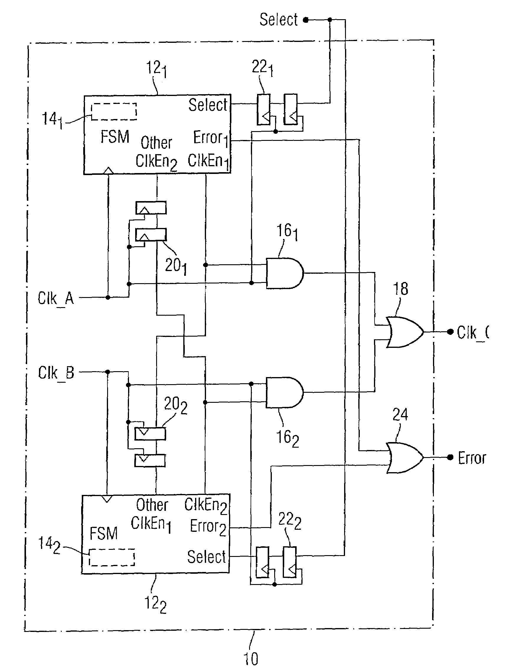
[0043]In FIG. 3 there is disclosed a block diagram of one embodiment of a digital clock switching circuit 10 according to the present invention. The digital clock switching circuit 10 is operable to deadlock-free switch the source of the digital clock for an integrated circuit. The digital clock switching circuit 10 comprises a first finite state machine 121 associated with a first clock source Clk_A, and a second finite state machine 122 associated with a second clock source Clk_B. As is apparent from FIG. 3, the finite state machines 121, 122 are connected to each other, via the signals ClkEn1, ClkEn2, Other ClkEn1, Other ClkEn2, in order to monitor the current state of the other finite state machine 122, 121, respectively. Each finite state machine 121, 122 has an input signal (Select) operable to control which clock source Clk_A;Clk_B that should be active and passed to a clock output Clk_Out of the digital clock switching circuit 10. Each finite state machine 121, 122 comprises...


PUM


Abstract

A digital clock switching circuit and method is disclosed and is operable to deadlock-free switch a digital clock source for an integrated circuit. The circuit includes a first finite state machine associated with a first clock source and a second finite state machine associated with a second clock source. The finite state machines are connected to each other and monitor the current state of the other finite state machine. Each finite state machine receives an input select signal to control which clock source should be active and passed to a clock output. Each finite state machine includes a counter, wherein the counter associated with the active clock source is initialized to a first predetermined value when the input select signal indicates a switching off of the active clock source. The finite state machine associated with the active clock source enters a CHECK state and varies a count at each clock cycle. If the other finite state machine verifies a presence of its clock source before the counter reaches a second predetermined value the switch of the active clock source is effected.

Description

REFERENCE TO RELATED APPLICATIONS[0001]This application claims the benefit of the priority date of European application 05 006 295.9, filed on Mar. 22, 2005, the contents of which are herein incorporated by reference in their entirety.FIELD OF THE INVENTION[0002]The present invention relates to a digital clock switching system operable to deadlock-free switch the source of a digital clock for an integrated circuit, and a method associated therewith.BACKGROUND OF THE INVENTION[0003]Most digital integrated circuits require a clock signal to synchronize their activity. Often, a circuit will be designed so that the clock signal can come from more than one source. For example, it may either be generated internally on the chip, or be supplied externally. The motivation for such a design is flexibility and reduced power consumption: in some applications, there could already be an externally generated clock available and so to generate another clock on-chip is wasteful of energy. In other a...

Claims


Application Information

Patent Timeline
Patent Type & Authority Patents(United States)
IPC IPC(8): G06F1/08
CPCH04J3/0688G06F1/08
Inventor LEWIS, MICHAEL
Owner INFINEON TECH AG
Why Eureka
Try Eureka