

Method of manufacturing a semiconductor device
a manufacturing method and semiconductor technology, applied in the direction of manufacturing tools, polishing compositions with abrasives, lapping machines, etc., can solve the problems of difficult to achieve a desired planarity, and the effect of preventing the formation of scratches
- Summary
- Abstract
- Description
- Claims
- Application Information
AI Technical Summary
Benefits of technology
Problems solved by technology
Method used
Image

Examples
example
[0044]Now referring to the accompanying drawings, the embodiments of the present invention will be described in further details. Hereafter, constituents employed in common in different drawings will be given an identical numeral, and description thereof may not be presented as the case may be.
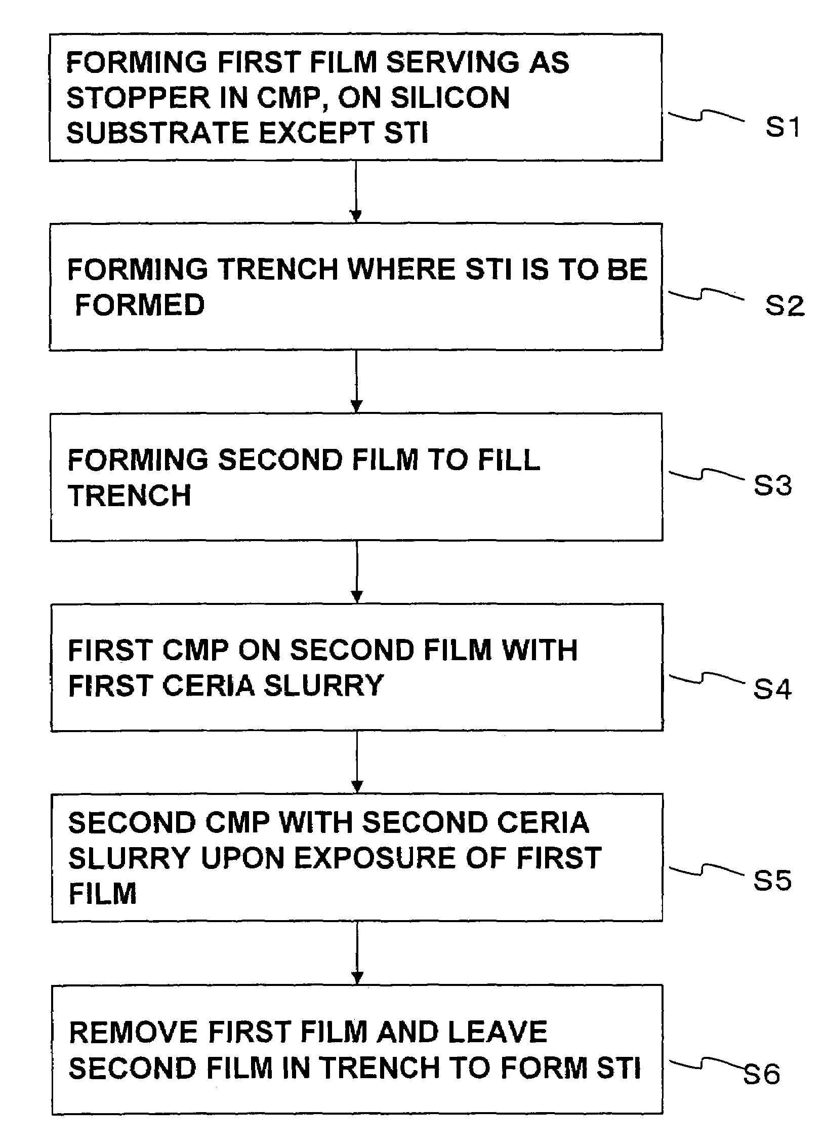
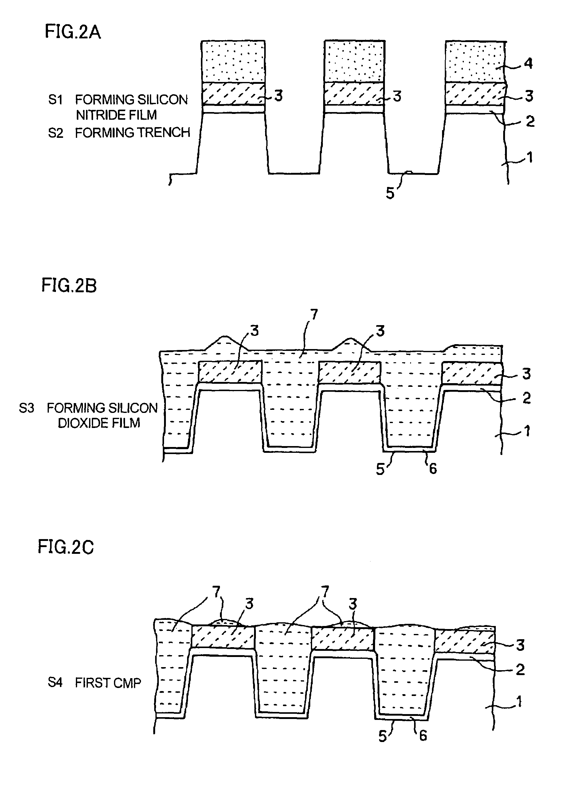
[0045]FIG. 1 is a flowchart describing a basic method of manufacturing a semiconductor device according to this embodiment, wherein the method is applied to formation of a shallow trench isolation (STI) region in a semiconductor device.
[0046]The manufacturing process of the STI shown in FIG. 1 includes a step S1 of forming a first film which serves as a stopper film in a CMP process, in a region on a silicon substrate other than an STI forming region, a step S2 of forming a trench in the STI forming region, a step S3 of forming a second film so as to fill the trench, a first CMP step S4 of performing a CMP on the second film utilizing a first ceria slurry, a second CMP step S5 of performing a C...
PUM
| Property | Measurement | Unit |
|---|---|---|
| diameter | aaaaa | aaaaa |
| thickness | aaaaa | aaaaa |
| thickness | aaaaa | aaaaa |
Abstract
Description
Claims
Application Information