Universal energy conditioning interposer with circuit architecture
What is Al technical title?
Al technical title is built by PatSnap Al team. It summarizes the technical point description of the patent document.
a technology of circuit architecture and energy conditioning, applied in the field of circuit interposers, can solve the problems of short product life cycle of electrical systems, unfavorable safety, and energy feed to ic chips having relatively high impedance, and achieve the effect of solving or reducing industry problems and obstacles, and being cost-effectiv
Inactive Publication Date: 2007-11-27
X2Y ATTENUATORS L L C
View PDF571 Cites 84 Cited by
Summary
Abstract
Description
Claims
Application Information
AI Technical Summary
This helps you quickly interpret patents by identifying the three key elements:
Problems solved by technology
Method used
Benefits of technology
[0015]The invention will also provide for simultaneous physical and electrical shielding to portions of an active chip structure as well as for internal propagating energies within the new structure by allowing predetermined, simultaneous energy interactions to take place between grouped and energized conductive pathways to be fed by pathways external to the embodiment elements.
[0016]This application expands upon this concept and further discloses a new circuit interposer comprising a multilayer, universal multi-functional, common conductive shield structure with conductive pathways that replaces multiple, discreet versions of various prior art devices with a single individual unit that provides a cost effective system of circuit protection and conditioning that will help solve or reduce industry problems and obstacles as described above.
[0019]It is an object of the invention to minimize or suppress unwanted electromagnetic emissions resulting from differential and common mode currents flowing within electronic pathways that come under the invention influence.
[0022]It is an object of the invention to be easily adapted to utilization with or without, one or more external conductive attachments to a conductive area located external to the originally manufactured invention. The external connection to a conductive area—can aid the invention embodiments in providing protection to electronic system circuitry.
Problems solved by technology
A main disadvantage of conventional approaches to interconnecting and packaging of IC chips in Multi Chip Modules (MCMs) arises from the thinness of the substrates used in traditional multichip modules results in the energy feeds to the IC chips having relatively high impedance.
This results in undesired noise, energy loss and excess thermal energy production.
These problems are relevant and can be critical to system integrity when routing or propagating energy along pathways though an interposer substrate.
Electrical systems have undergone short product life cycles over the last decade.
However, the evolvement of passive electronic componentry has not kept pace.
During this same period, however, passive component technologies have failed to keep up with these new breakthroughs and have produced only incremental changes in composition and performance.
Attempts to line condition propagating energy with prior art components has led to increased levels of interference in the form of EMI, RFI, and capacitive and inductive parasitics.
These increases are due in part to manufacturing imbalances and performance deficiencies of the passive components that create or induce interference into the associated electrical circuitry.
Other sources of EMI interference are generated from the active silicon components as they operate or switch.
These problems such as SSO are notorious causes of circuit disruptions.
Other problems include unshielded and parasitic energy that freely couples upon or onto the electrical circuitry and generates significant interference at high frequencies.
Method used
Image
Click on the blue label to locate the original text in one second.
Reading with bidirectional positioning of images and text.
Examples
Embodiment Construction
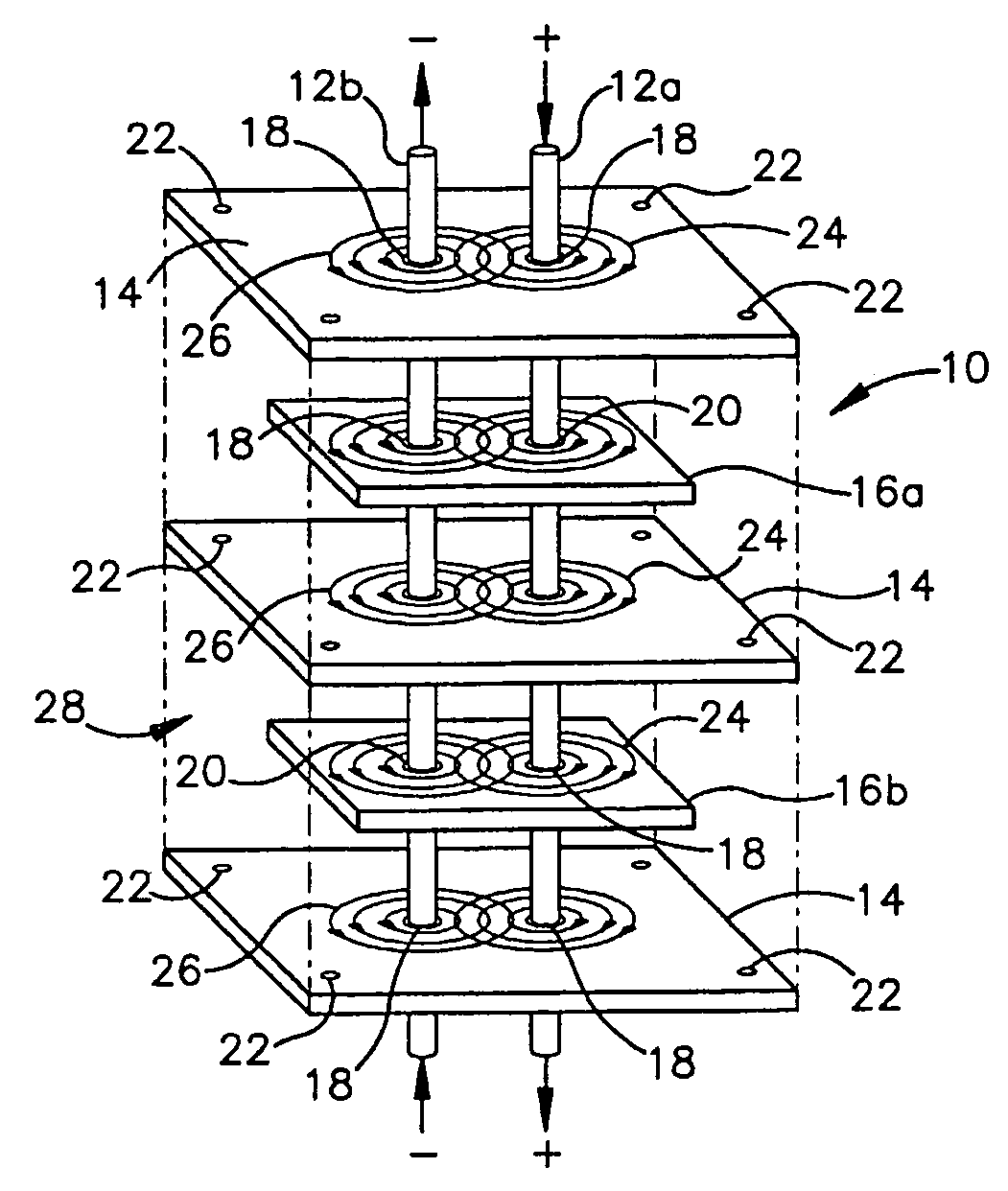
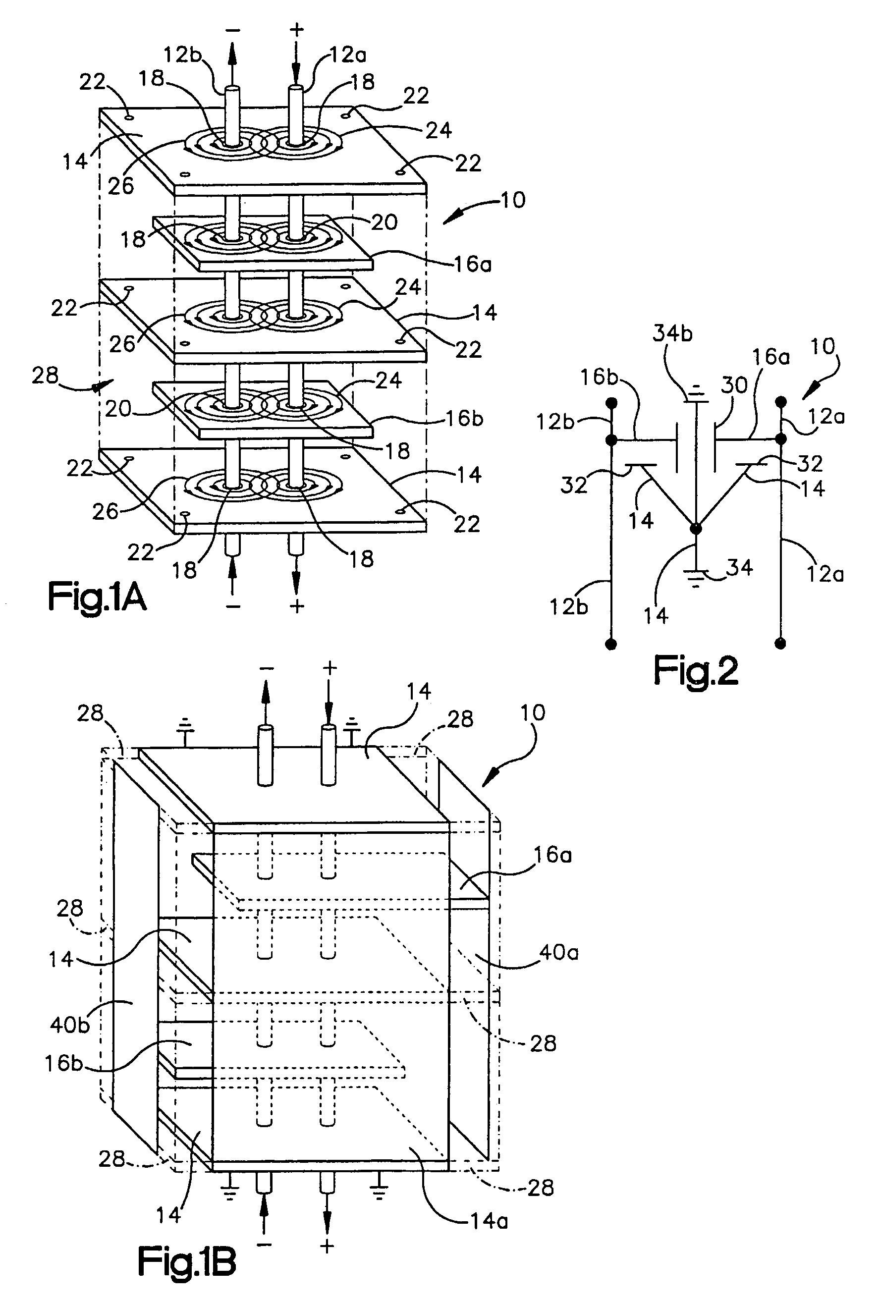
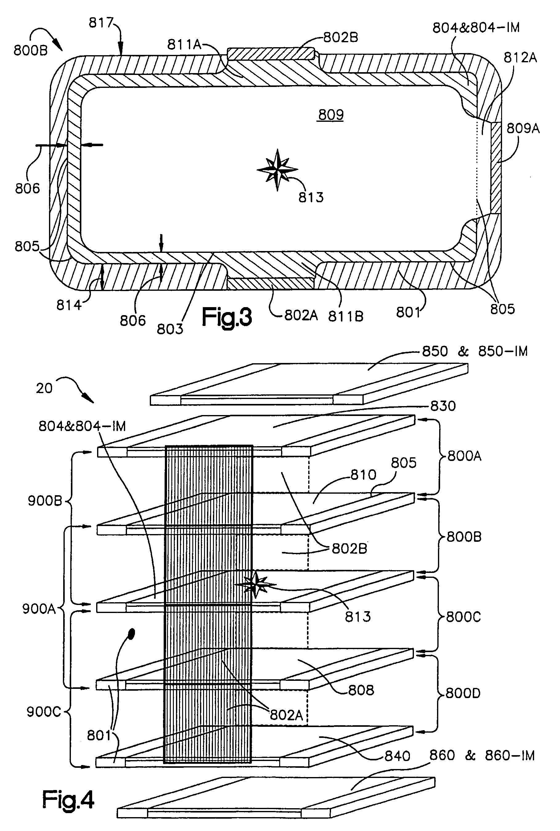
[0044]As used herein, the acronym terms “UECICA” will be used to mean a universal energy conditioning interposer with circuit architecture for energy and EMI conditioning and protection within the scope of the present invention and refers to all types of discrete versions of the device.
[0045]In addition, as used herein, the acronym term “AOC” for the words “predetermined area or space of physical convergence or junction” which is defined as the physical boundary of manufactured-together invention elements. Non-energization and energization are defined as the range or degree to which electrons within the “AOC” of either discrete or non-discrete versions of UECICA are in motion and are propagating to and / or from an area located outside the pre-determined in a balanced manner.
[0046]U.S. Pat. No. 6,018,448, which is a continuation-in-part of application Ser. No. 09 / 008,769 filed Jan. 19, 1998, now issued as U.S. Pat. No. 6,097,581, which is a continuation-in-part of application Ser. No....
PUM
Property
Measurement
Unit
operating frequency
aaaaa
aaaaa
capacitance
aaaaa
aaaaa
series resonant frequencies
aaaaa
aaaaa
Abstract
The present invention relates to an interposer substrate for interconnecting between active electronic componentry such as but not limited to a single or multiple integrated circuit chips in either a single or a combination and elements that could comprise of a mounting substrate, substrate module, a printed circuit board, integrated circuit chips or other substrates containing conductive energy pathways that service an energy utilizing load and leading to and from an energy source. The interposer will also possess a multi-layer, universal multi-functional, common conductive shield structure with conductive pathways for energy and EMI conditioning and protection that also comprise a commonly shared and centrally positioned conductive pathway or electrode of the structure that can simultaneously shield and allow smooth energy interaction between grouped and energized conductive pathway electrodes containing a circuit architecture for energy conditioning as it relates to integrated circuit device packaging. The invention can be employed between an active electronic component and a multilayer circuit card. A method for making the interposer is not presented and can be varied to the individual or proprietary construction methodologies that exist or will be developed.
Description
[0001]This application is a continuation of application Ser. No. 10 / 237,079, filed Sep. 9, 2002, now U.S. Pat. No. 7,110,227 which is a continuation-in-part of Ser. No. 09 / 632,048, filed Aug. 3, 2000, now U.S. Pat. No. 6,738,249 which is a continuation-of-part of application Ser. No. 09 / 600,530, filed Jul. 18, 2000, now U.S. Pat. No. 6,498,710 which is a continuation-in-part of application Ser. No. 09 / 594,447 filed Jun. 15, 2000, now U.S. Pat. No. 6,636,406 which is a continuation-in-part of application Ser. No. 09 / 579,606 filed May 26, 2000, now U.S. Pat. No. 6,373,673 which is a continuation-in-part of application Ser. No. 09 / 460,218 filed Dec. 13, 1999, now U.S. Pat. No. 6,331,926 which is a continuation of application Ser. No. 09 / 056,379 filed Apr. 7, 1998, now issued as U.S. Pat. No. 6,018,448, which is a continuation-in-part of application Ser. No. 09 / 008,769 filed Jan. 19, 1998, now issued as U.S. Pat. No. 6,097,581, which is a continuation-in-part of application Ser. No. 08 / ...
Claims
Application Information
Patent Timeline
Application Date:The date an application was filed.
Publication Date:The date a patent or application was officially published.
First Publication Date:The earliest publication date of a patent with the same application number.
Issue Date:Publication date of the patent grant document.
PCT Entry Date:The Entry date of PCT National Phase.
Estimated Expiry Date:The statutory expiry date of a patent right according to the Patent Law, and it is the longest term of protection that the patent right can achieve without the termination of the patent right due to other reasons(Term extension factor has been taken into account ).
Invalid Date:Actual expiry date is based on effective date or publication date of legal transaction data of invalid patent.