Synchronous pseudo static random access memory

a random access and memory technology, applied in the field of synchronous pseudo random access memory, can solve the problems of performance degradation of the memory device and increase the current consumption of the refresh operation, and achieve the effect of improving the operation efficiency

Inactive Publication Date: 2007-11-27
SK HYNIX INC
View PDF8 Cites 13 Cited by
  • Summary
  • Abstract
  • Description
  • Claims
  • Application Information

AI Technical Summary

Benefits of technology

[0016]It is, therefore, an object of the present invention to provide a latency control circuit for use in a synchronous PSRAM for improving an operation efficiency.

Problems solved by technology

However, when a refresh period becomes smaller, the performance degradation of the memory device occurs because an external device is not able to access to the memory device while the refresh operation is performed.
Further, when the refresh operation is performed more frequently, the current consumption for the refresh operation is increased.
Nevertheless, the conventional PSRAM always includes a latency for the refresh operation because the initial latency is fixed.

Method used


Image

  • Synchronous pseudo static random access memory
  • Synchronous pseudo static random access memory
  • Synchronous pseudo static random access memory

Examples


Embodiment Construction

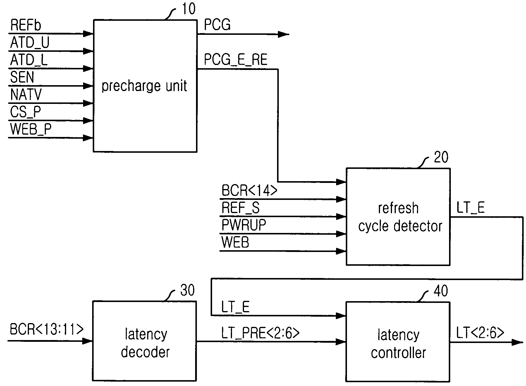
[0027]Hereinafter, a latency control circuit for use in a synchronous pseudo static random access memory (PSRAM) in accordance with the present invention will be described in detail referring to the accompanying drawings.

[0028]FIG. 3 is a block diagram describing the latency control circuit for use in a synchronous PSRAM in accordance with an embodiment of the present invention.

[0029]As shown, the latency control circuit includes a precharge unit 10, a refresh cycle detector 20, a latency decoder 30, and a latency controller 40.

[0030]The precharge unit 10 receives a refresh signal REFb, an upper and a lower address detection signals ATD_U and ATD_L, a sense signal SEN, a normal active signal NATV, a chip selection signal CS_P, and a first write enable signal WEB_P to thereby output a precharge signal PCG and a precharge reset signal PCG_E_RE. Herein, the chip selection signal CS_P is activated as a logic high level and the write enable signal WEB_P is pulse signal generated when a w...


PUM


Abstract

A latency control circuit for use in a semiconductor memory device includes a precharge unit for outputting a precharge reset signal based on a refresh signal and a normal active signal, wherein the precharge reset signal is used for extending a latency during a burst read period which includes a refresh cycle; a refresh cycle detector for detecting the refresh cycle in response to a latency setting signal and the precharge reset signal to thereby output a latency extension signal; a latency decoder for decoding an external address to thereby output a plurality of preliminary latency signals; and a latency controller for outputting a plurality of latency signals in response to the preliminary latency signal and the latency extension signal.

Description

FIELD OF THE INVENTION[0001]The present invention relates to a synchronous pseudo random access memory (PSRAM); and, more particularly, to a synchronous PSRAM for improving an operation efficiency by varying the latency according to the refresh operation.DESCRIPTION OF RELATED ARTS[0002]Generally, a semiconductor memory device includes a plurality of memory cells, a plurality of sense amplifiers for driving the memory cells, a row decoder, and a column decoder. A data stored in a predetermined memory cell is selected by using the row decoder and the column decoder and, then, amplified by the sense amplifier.[0003]The memory cell of a dynamic random access memory (DRAM) is provided with one cell transistor performing a switching operation and one capacitor storing the data. Meanwhile, the data stored in the capacitor is discharged because of a leakage current occurring at a PN junction of the cell transistor. Therefore, a refresh operation is performed to thereby maintain the origina...

Claims


Application Information

Patent Timeline
Patent Type & Authority Patents(United States)
IPC IPC(8): G11C7/00
CPCG11C11/40615G11C11/406G11C7/12G11C7/22G11C11/4094G11C11/4076G11C11/34
Inventor LEE, YIN-JAE
Owner SK HYNIX INC
Why Eureka
Try Eureka