System and method for automatic insertion of on-chip decoupling capacitors

a technology of decoupling capacitors and on-chip decoupling, applied in the field of automatic insertion of on-chip decoupling capacitors, can solve problems such as the generation of voltage noise-maps for integrated circuits

Inactive Publication Date: 2007-11-27
GOOGLE LLC
View PDF4 Cites 9 Cited by
  • Summary
  • Abstract
  • Description
  • Claims
  • Application Information

AI Technical Summary

Problems solved by technology

This voltage noise distribution may be generated using any of a number of different known mechanisms and generally results in a voltage noise-map being generated for the integrated circuit.

Method used


Image

  • System and method for automatic insertion of on-chip decoupling capacitors
  • System and method for automatic insertion of on-chip decoupling capacitors
  • System and method for automatic insertion of on-chip decoupling capacitors

Examples


Embodiment Construction

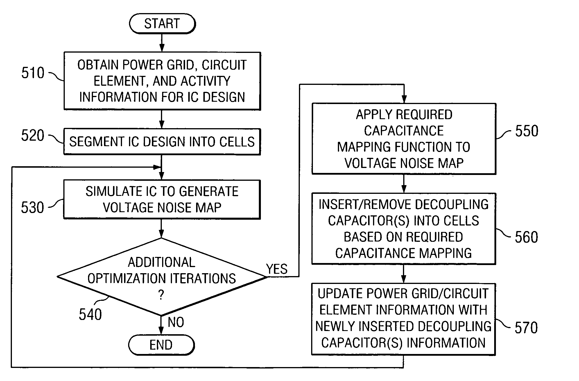
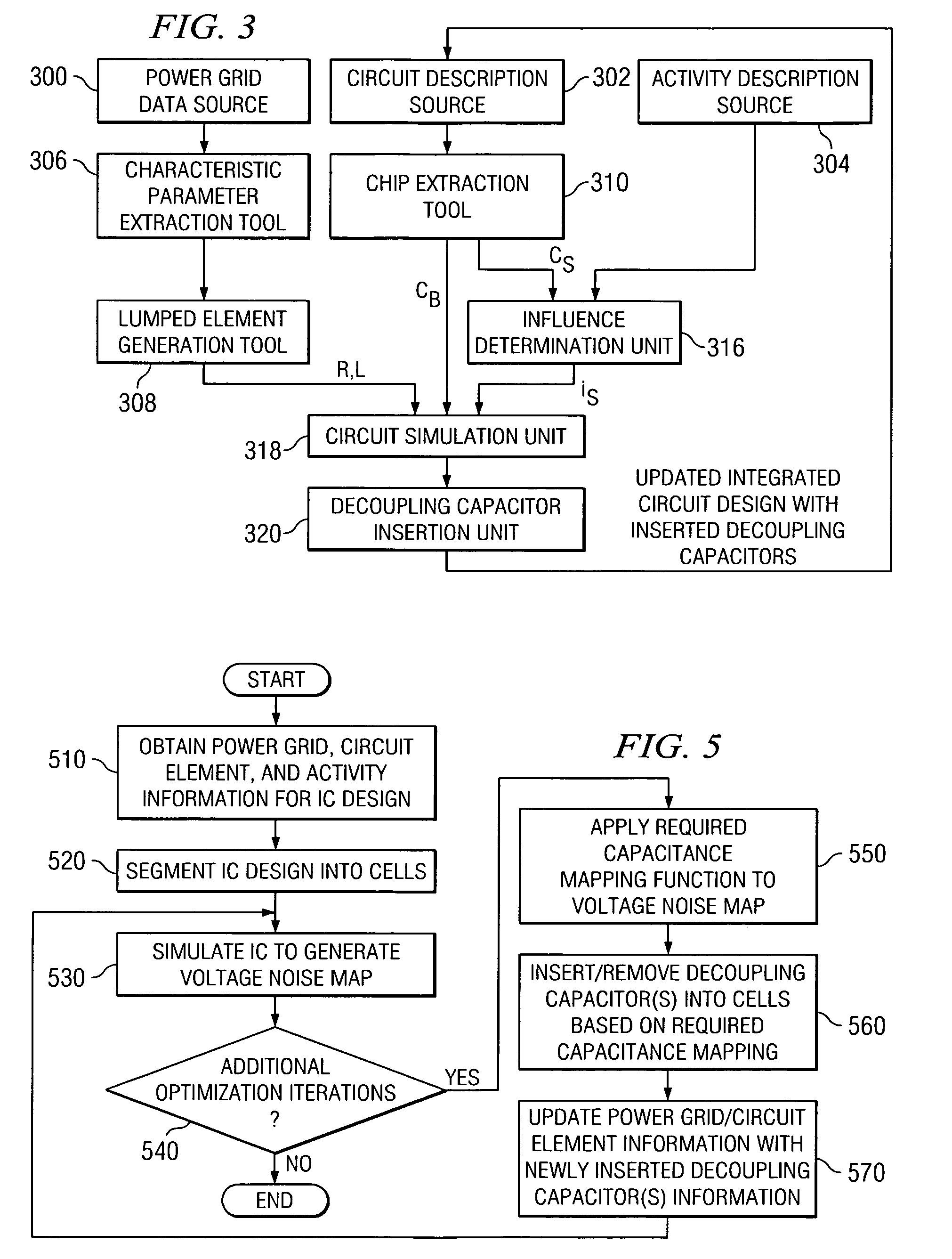
[0019]The present invention provides a mechanism for determining the required capacitance for portions of an integrated circuit design and thus, the type and location for insertion of decoupling capacitors, in an integrated circuit design. The mechanism of the present invention is preferably implemented as part of an integrated circuit design system. As such, the present invention is preferably implemented in a computing system in which integrated circuit design software is executed. FIG. 1 is provided as one example of a computer system in which aspects of the present invention may be implemented. However, it should be appreciated that FIG. 1 is only exemplary and is not intended to state or imply any limitation with regard to the type or configuration of computer systems in which the present invention may be implemented.

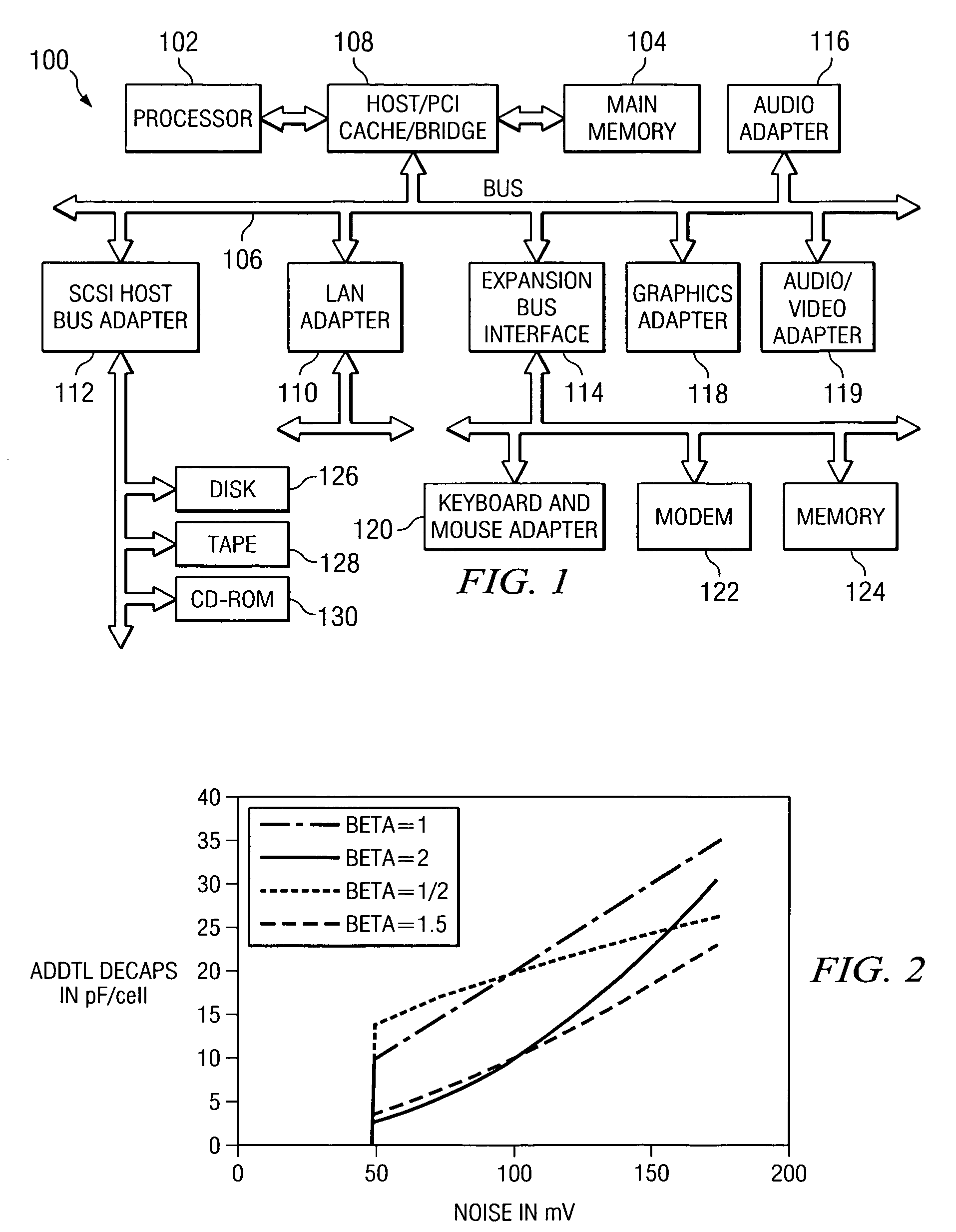
[0020]With reference now to FIG. 1, a block diagram of a data processing system is shown in which the present invention may be implemented. Data processing system ...


PUM


Abstract

A system and method for automatic insertion of on-chip decoupling capacitors are provided. With the system and method, an integrated circuit design is partitioned into cells and the noise distribution per cell of an integrated circuit is determined. This noise distribution may be generated using any of a number of different known mechanisms and generally results in a noise-map being generated for the integrated circuit. Thereafter, a mapping function is applied to the noise map for each cell to determine a required capacitance for the cells of the integrated circuit. From this required capacitance per cell, the necessary decoupling capacitors may be identified as well as the location for insertion of these decoupling capacitors. In a similar manner, decoupling capacitors may be removed from cells of the integrated circuit based upon the determined required capacitance per cell.

Description

BACKGROUND OF THE INVENTION[0001]1. Technical Field[0002]The present invention relates generally to the field of design automation and computer-aided design (CAD) in the area of development of integrated circuits. More specifically, the present invention provides a system and method for automatic insertion of on-chip decoupling capacitors.[0003]2. Description of Related Art[0004]Complementary Metal Oxide Semiconductor (CMOS) circuit technology of today and its application in synchronously switching digital Very Large Scale Integration (VLSI) systems imposes high frequency current changes on the associated power distribution network formed by power supply wiring and decoupling capacitors. The reason lies in the semiconductor fabrication technology. CMOS circuit technology uses a combination of n- and p-doped semiconductor material to achieve low power dissipation. Any path through a gate through which current can flow includes both n- and p-type transistors. Only one type is turned o...

Claims


Application Information

Patent Timeline
Patent Type & Authority Patents(United States)
IPC IPC(8): G06F17/50
CPCG06F17/5045G06F2217/78G06F30/30G06F2119/06
Inventor HARIDASS, ANANDHUBER, ANDREASKLINK, ERICHSUPPER, JOCHEN
Owner GOOGLE LLC
Why Eureka
Try Eureka