Systems and methods for modifying a reticle's optical properties

a technology of optical properties and reticles, applied in the direction of photomechanical treatment originals, instruments, nuclear engineering, etc., can solve the problems of circuits decreasing, defects or marginalities in the features formed on the reticles becoming increasingly important, circuits reducing, etc., to achieve significant flexibility and more deviations

Inactive Publication Date: 2007-12-04
KLA TENCOR TECH CORP
View PDF8 Cites 19 Cited by
  • Summary
  • Abstract
  • Description
  • Claims
  • Application Information

AI Technical Summary

Benefits of technology

[0012]Embodiments of the present invention allow one to adjust optical properties of a reticle using an optical beam, thus, providing significant flexibility for correcting errors produced by the reticle or simply optimizing the reticle's properties. Embodiments for widening the process window of the reticle by locally or globally changing optical properties on the reticle allow more deviations in the lithography process to occur without causing harm to the printed wafer.

Problems solved by technology

Consequently, defects that are formed on the wafer during lithography may be particularly problematic for the integrated circuit manufacturing process.
However, as the dimensions of integrated circuits decrease and the patterns being transferred from the reticle to the wafer become more complex, defects or marginalities in the features formed on the reticle become increasingly important.
In particular, if the pattern is not formed on the reticle, such discrepancies increasingly produce defects on the wafer as the dimension of the pattern decrease and the complexity of the pattern increases.
In addition, marginalities in the reticle design may cause the design to print incorrectly on the wafer.
These efforts are relatively complex and difficult due, at least in part, to the fact that not all discrepancies or marginalities in the pattern formed on the reticle (as compared to the ideal pattern) will cause errors on the wafer that will adversely affect the integrated circuit.
In other words, some error in the pattern formed on the reticle may not produce defects on the wafer at all or may produce defects on the wafer that will not reduce the performance characteristics of the integrated circuit.

Method used


Image

  • Systems and methods for modifying a reticle's optical properties
  • Systems and methods for modifying a reticle's optical properties
  • Systems and methods for modifying a reticle's optical properties

Examples


Embodiment Construction

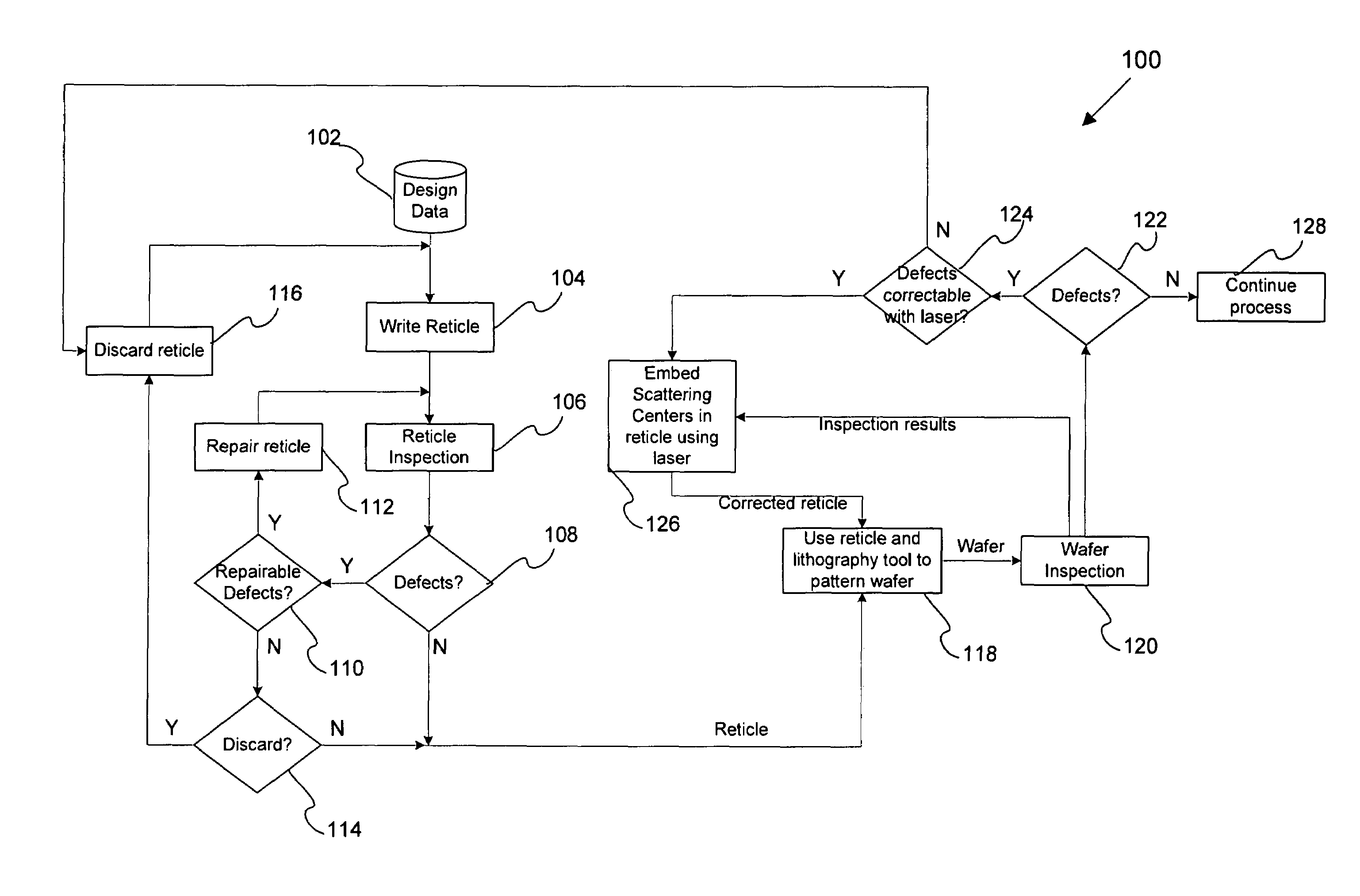
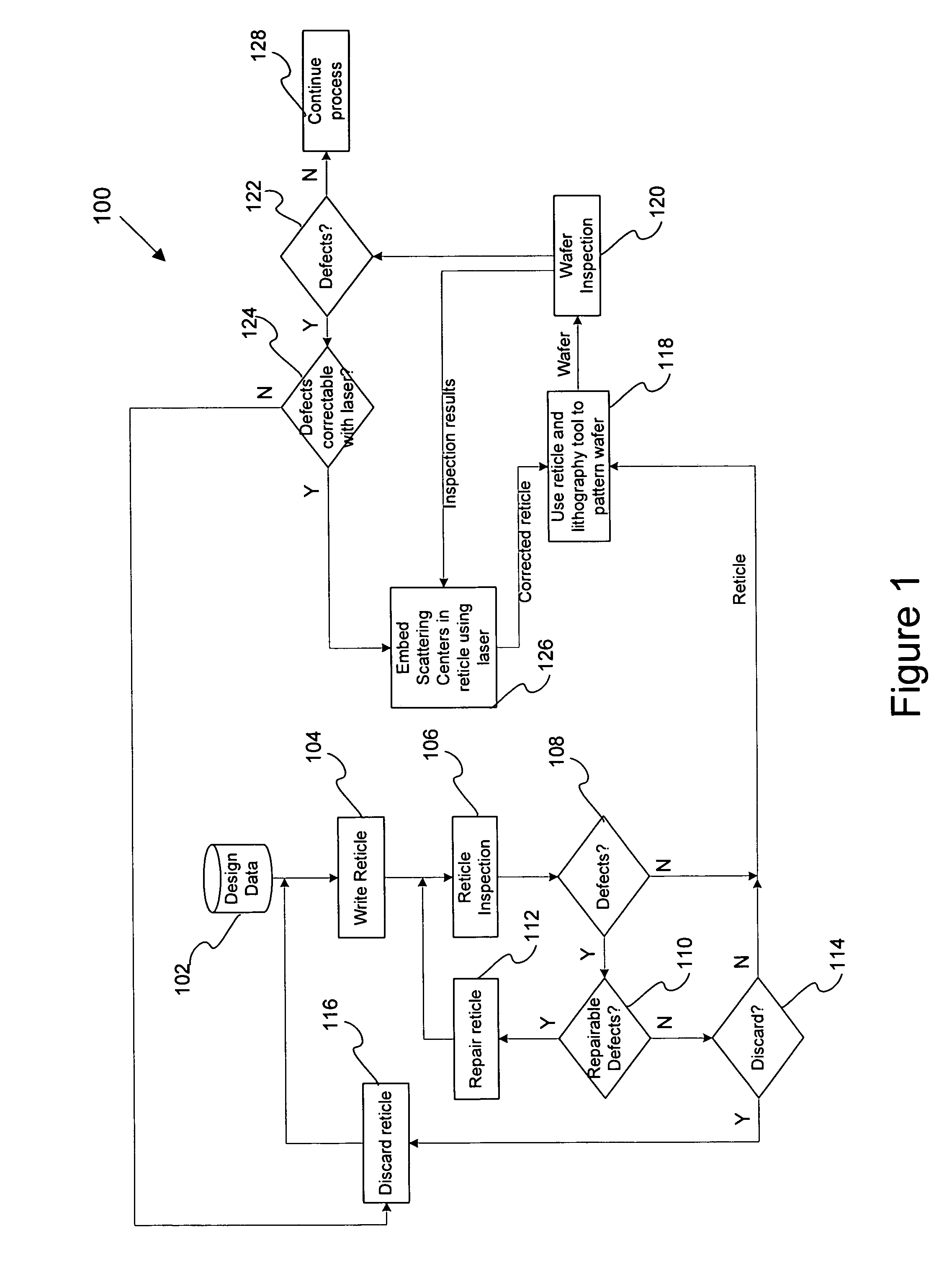
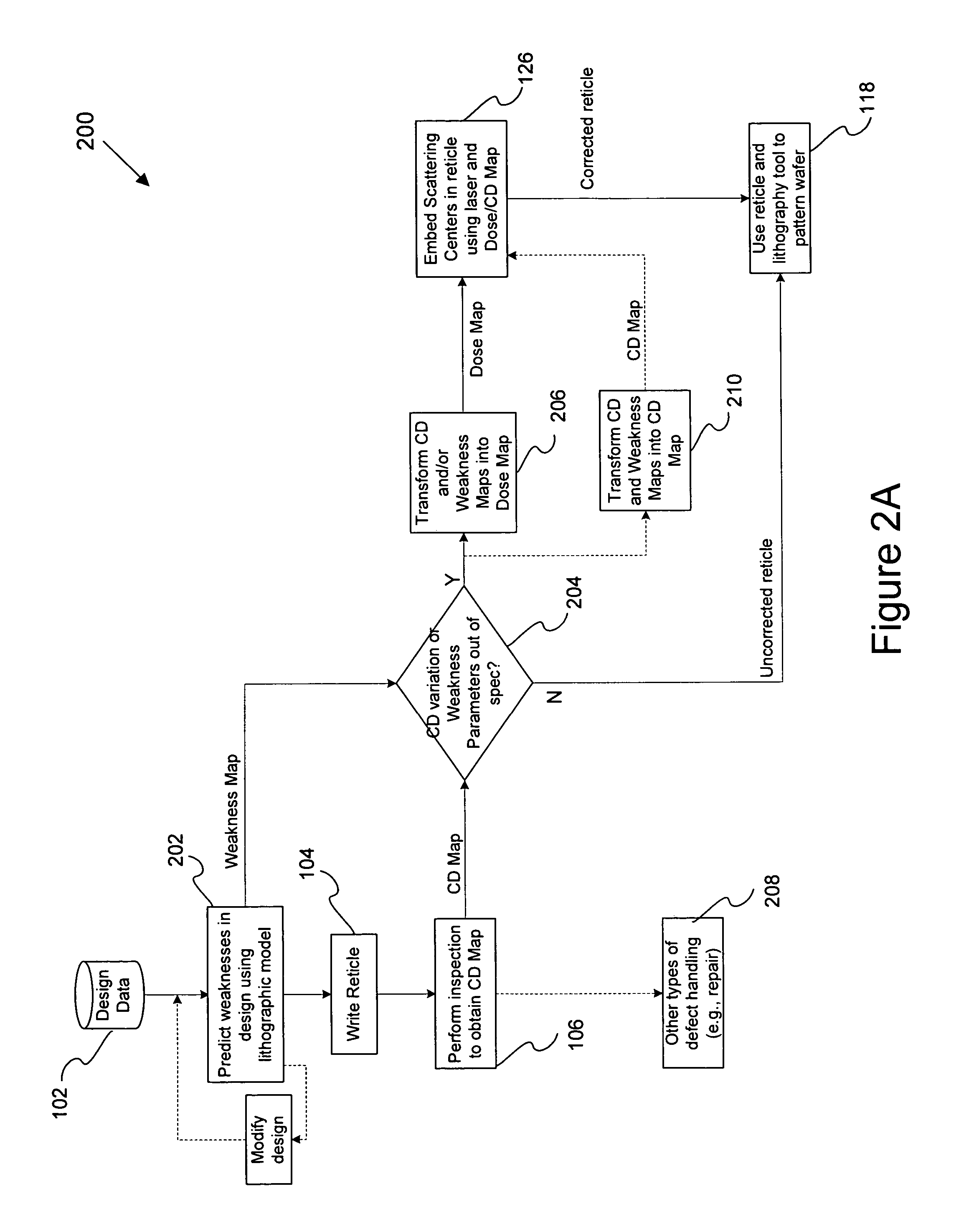
[0031]Reference will now be made in detail to a specific embodiment of the invention. An example of this embodiment is illustrated in the accompanying drawings. While the invention will be described in conjunction with this specific embodiment, it will be understood that it is not intended to limit the invention to one embodiment. On the contrary, it is intended to cover alternatives, modifications, and equivalents as may be included within the spirit and scope of the invention as defined by the appended claims. In the following description, numerous specific details are set forth in order to provide a thorough understanding of the present invention. The present invention may be practiced without some or all of these specific details. In other instances, well known process operations have not been described in detail in order not to unnecessarily obscure the present invention.

[0032]A “reticle” or a “mask” is generally defined as a substantially transparent substrate having substanti...


PUM

PropertyMeasurementUnit
distanceaaaaaaaaaa
distanceaaaaaaaaaa
optical propertyaaaaaaaaaa

Abstract

Disclosed are systems and methods for modifying a reticle. In general, inspection results from a plurality of wafers or prediction results from a lithographic model are used to individually decrease the dose or any other optical property at specific locations of the reticle. In one embodiment, any suitable optical property of the reticle is modified by an optical beam, such as a femto-second laser, at specific locations on the reticle so as to widen the process window for such optical property. Examples of optical properties include dose, phase, illumination angle, and birefringence. Techniques for adjusting optical properties at specific locations on a reticle using an optical beam may be practiced for other purposes besides widening the process window.

Description

RELATED APPLICATION DATA[0001]The present application claims priority under 35 U.S.C. 119(e) to U.S. Provisional Patent Application No. 60 / 671,293, filed Apr. 13, 2005, and U.S. Provisional Patent Application No. 60 / 758,576, filed Jan. 11, 2006, the entire disclosures of both which are incorporated herein by reference for all purposes.FIELD OF THE INVENTION[0002]The invention pertains in general to integrated circuit design and fabrication, and in particular to mitigating actual or potential variations on a patterned wafer.BACKGROUND[0003]Fabricating semiconductor devices such as logic and memory devices typically includes processing a substrate such as a semiconductor wafer using a number of semiconductor fabrication processes to form various features and multiple levels of the semiconductor devices. For example lithography is a semiconductor fabrication process that involves transferring a pattern from a reticle to a resist arranged on a semiconductor wafer. Additional examples of...

Claims


Application Information

Patent Timeline
Patent Type & Authority Patents(United States)
IPC IPC(8): G03F9/00
CPCG03F1/72G06K9/2063G03F1/84Y10S430/146G06V10/225
Inventor WATSON, STERLING G.LEVY, ADYMACK, CHRIS A.STOKOWSKI, STANLEY E.SAIDIN, ZAIN K.ZURBRICK, LARRY S.
Owner KLA TENCOR TECH CORP
Why Eureka
Try Eureka