Method of managing a multi-bit cell flash memory with improved reliablility and performance

a multi-bit cell flash memory and reliablility technology, applied in the field of flash memory, can solve the problems of memory block having to be erased, drawbacks of using mbc flash, and misnomer term

Active Publication Date: 2007-12-11
WESTERN DIGITAL ISRAEL LTD
View PDF17 Cites 105 Cited by
  • Summary
  • Abstract
  • Description
  • Claims
  • Application Information

AI Technical Summary

Problems solved by technology

A limitation of flash memory is that while flash memory can be read or programmed, for instance in NOR flash a byte or word at a time in a random access fashion, a block of memory must be erased at the same time.
The latter term is a misnomer, as the implementations do not necessarily support “files”, in the sense that files are used in operating systems or personal computers, but rather support block device interfaces similar to those exported by hard disk software drivers.
However, there are drawbacks to using MBC flash.
Average read and write times of MBC memories are longer than of SBC memories, resulting in worse performance.
Also, the reliability of MBC is lower than SBC.
Thus, a disturbance in the threshold voltage (e.g. leakage of stored charge causing a threshold voltage drift or interference from operating neighboring cells) that are insignificant in SBC because of the large gap between the two states, may cause an MBC cell to move from one state to another, resulting in an erroneous bit.
The end result is a lower performance specification of MBC cells in terms of data retention time or the endurance of the device to many write / erase cycles.
While an error in the user data does not damage the flash management system, an error in the control information might result in the loss of a whole sector, a whole block, or (in extreme cases) even the whole disk contents.
Prior art flash memory systems do not support separating “modes” between user data and control information.
Prior art flash devices do not support a single writing operation which writes some memory cells using MBC mode and other memory cells using SBC mode, because much of the internal circuitry of the flash device which carries out the writing operation is shared between all the cells being written together, and the prior art circuitry cannot act at the same time in two different modes.
Secondly, the flash device must be instructed (by the controller of the flash system) in which mode, MBC or SBC, the page is programmed, and the current interfaces of existing flash devices do not support mixing modes within the same basic operation.

Method used


Image

  • Method of managing a multi-bit cell flash memory with improved reliablility and performance
  • Method of managing a multi-bit cell flash memory with improved reliablility and performance
  • Method of managing a multi-bit cell flash memory with improved reliablility and performance

Examples


embodiment 1

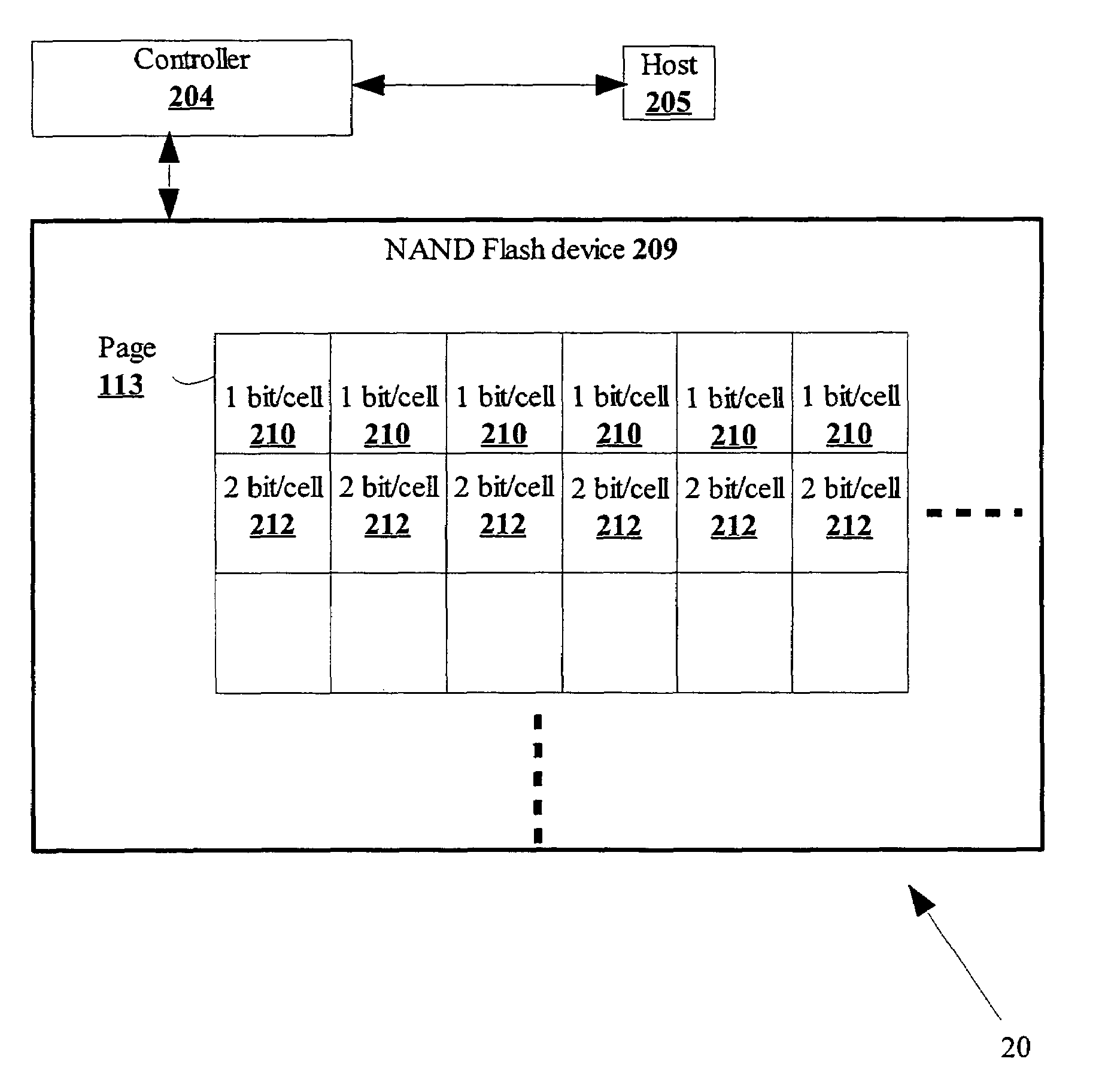
[0048]The first embodiment of the present invention is to write the control information and the user data using MBC mode, but still get improved reliability (but not improved read performance) similar to SBC mode. For this to be achieved we restrict the use of the memory cells used for storing the control information to storing just a single bit worth of information each, and not utilize the extra bits that can be stored in these cells when using MBC mode.

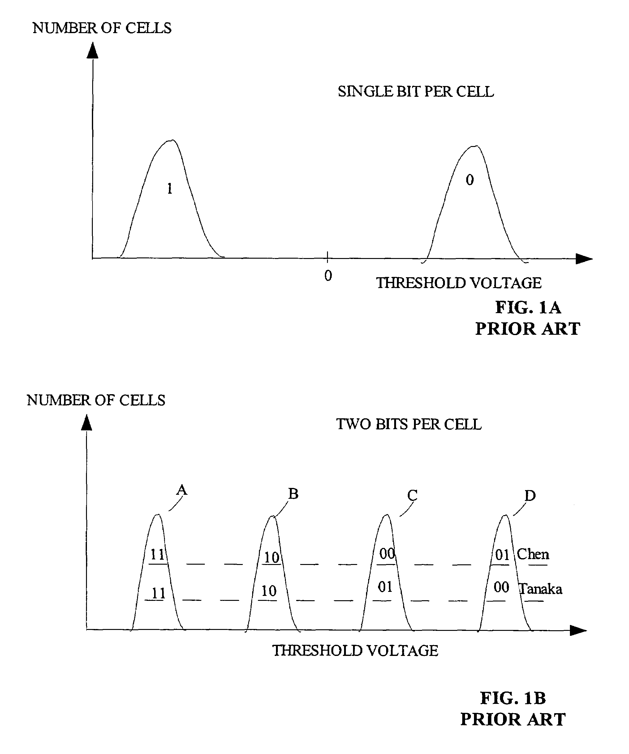
[0049]As already explained above, the reason for lower reliability when using MBC mode compared to SBC mode, is the smaller gap between the states of the cell. Thus it is more probable for a cell to erroneously change its state and thus represent incorrect value for one or more of the stored bits. But suppose we use the same cell in a restricted way—only the states “11” and “01” are used, using the Chen coding convention. As can be seen in FIG. 1B, this is the pair of states with largest separation on the threshold voltage axis. Th...

embodiment 2

A Further Improvement: Embodiment 2

[0075]The first embodiment presented above provides for storing control information with high reliability, but does not address the need for storing control information so as to provide better read performance. A second embodiment of the present invention addresses this need too and supports both the reliability and performance goals. The second embodiment, as opposed to the first embodiment requires a special read command provided by the flash device.

[0076]This second embodiment uses the same principles as the first embodiment, also relying on storing the control information with each bit allocated a separate cell, and picking the two furthest separated states of a MBC cell for representing the single bit stored in the cell. When it comes to writing, the second embodiment of the present invention is completely identical to the first embodiment. The only difference is in how reading is done. While the first embodiment employs standard MBC-mode read...

embodiment 3

An Additional Improvement: Embodiment 3

[0080]The first and second embodiments presented above provide for the reliable storage of control information by storing each control information bit in a separate cell, and choosing the right-most state of the MBC cell to represent a “0”. Choosing the “right-most” state provides for the widest separation between the two valid states and therefore has the lowest probability of the cell drifting with time towards the “1” state and generating an error.

[0081]While using the “right-most” state is the best counter-measure for defending against errors caused by charge leakage from the floating gate of the cells, there is another potential source of errors known as “over programming” in NAND flash devices. For understanding the architecture of the cells array in NAND devices and the reasons for the existence of the over programming effect, one is referred to Chen et al. U.S. Pat. No. 6,522,580 entitled “Operating techniques for reducing effects of co...


PUM


Abstract

A method of storing data by providing a flash memory device including a plurality of memory cells; each of the memory cells is capable of storing data bits. First data bits are stored into memory cells used for storing M bits per cell, the memory cells are allocated to a page of the memory. Second data bits are stored into other memory cells, the other memory cells used for storing N bits per cell are allocated to the page and upon storing of the first data bits and upon storing the second data bits, the page uses at the same time at least one of the memory cells with M bits per cell and at least one of the other memory cells with N bits per cell with N less than M.

Description

CROSS REFERENCE TO RELATED APPLICATIONS[0001]This application claims the benefit from U.S. provisional application 60 / 642,055 filed 10 Jan. 2005 by the present inventors.FIELD AND BACKGROUND OF THE INVENTION[0002]The present invention relates to flash memories and, more particularly, to a flash memory with memory cells programmed with more than one bit per cell. Particularly, the present invention includes storing in a single page of the memory more than one density (bits / cell).[0003]Flash memory is a type of non-volatile memory. Non-volatile memory stores information on a silicon chip in a way that does not need power to maintain the information in the chip. If power to the chip is turned off, the information is retained without consuming any power. Flash memory is made in different forms including NOR flash and NAND flash. The names refer to the similarity of the interconnections between storage cells in the two types of flash memory to the well-known NOR and NAND logic circuits. ...

Claims


Application Information

Patent Timeline
Patent Type & Authority Patents(United States)
IPC IPC(8): G11C16/04
CPCG11C11/5621G11C16/0483G11C11/5628G11C2211/5641G11C16/10
Inventor LASSER, MENAHEMMURIN, MARK
Owner WESTERN DIGITAL ISRAEL LTD
Why Eureka
Try Eureka