Method for heat-treating silicon wafer and silicon wafer

a technology of heat-treating silicon and silicon wafers, which is applied in the direction of crystal growth process, after-treatment details, polycrystalline material growth, etc., can solve the problems of deterioration in gate oxide integrity and other electrical characteristics, no effective means for removing heavy metal impurities, and contamination of silicon wafer surface with impurities present in a parent material, etc., to achieve adequate suppression of iron contamination and high quality

Active Publication Date: 2007-12-25
SUMCO CORP
View PDF7 Cites 2 Cited by
  • Summary
  • Abstract
  • Description
  • Claims
  • Application Information

AI Technical Summary

Benefits of technology

[0017]In light of the above problems, it is an object of the present invention to provide silicon wafers having a defect-free layer in a surface layer portion of the silicon wafer and having a low heavy metal contamination (iron contamination) in a wafer surface. Another object of the present invention is to provide a method for heat-treating a silicon wafer for obtaining such silicon wafers.
[0018]As a result of extensive investigations conducted in order to achieve these objects, we have discovered that iron contamination in the wafer surface can be suppressed by keeping a rate for lowering a temperature low in a specific ambient gas atmosphere during a step of lowering a temperature following a high-temperature heat treatment.
[0020]According to the present invention, a sufficient defect-free layer can be achieved in the surface layer portion of the wafer, and iron contamination in the wafer surface can be suppressed. Although the reason for the decrease in iron contamination is not yet understood, in the case in which a temperature is lowered at a rate greater than 2° C. / min in a nitrogen-gas-containing ambient atmosphere, this desirable effect is not obtained; nor is this effect obtained in the case in which a temperature is lowered at a rate of 2° C. / min or less in an ambient gas atmosphere other than a nitrogen-gas-containing ambient atmosphere. We have found that this effect occurs only when both conditions of the gas ambient atmosphere and the rate for lowering a temperature are completed.
[0022]In the method for heat-treating a silicon wafer of the present invention, the lowering a temperature at a rate of 2° C. / min or less in a nitrogen-gas-containing ambient atmosphere may be carried out in a temperature range of 700° C. or less during the process of lowering a temperature. This enables iron contamination of the wafer surface to be further suppressed.
[0026]According to the present invention, by subjecting a silicon wafer to a high-temperature heat treatment in an ambient gas atmosphere of hydrogen gas, argon gas or a gas mixture thereof, and then lowering a temperature at a rate of 2° C. / min or less in a nitrogen-gas-containing ambient atmosphere in a portion or all of a process of lowering a temperature to a wafer removal temperature, a sufficiently defect-free layer can be achieved in the surface layer portion of the wafer and iron contamination can be adequately suppressed in the wafer surface. Moreover, although the wafer of the present invention is an annealed wafer heat-treated at a high temperature, it is of a high quality characterized by an average iron concentration in the silicon wafer surface of 1×10¹⁰ atoms / cm3 or less, enabling remarkable improvements to be made in device characteristics.

Problems solved by technology

When present in the surface layer portion of the wafer where devices are fabricated, these defects cause a deterioration in the gate oxide integrity and other electrical characteristics.
In a high-temperature heat treatment in a hydrogen gas-containing ambient atmosphere, it is well-known that a reducing action of the hydrogen gas etches surfaces of a quartz reaction tube and a wafer boat (which is made of quartz, silicon or SiC), thereby, during the heat treatment, a silicon wafer surface is contaminated with impurities present in a parent material, especially heavy metals such as iron, copper and nickel.
There is no effective means for removing heavy metal impurities once they have diffused to the wafer surface as a result of the high-temperature heat treatment.

Method used


Image

  • Method for heat-treating silicon wafer and silicon wafer
  • Method for heat-treating silicon wafer and silicon wafer

Examples


examples

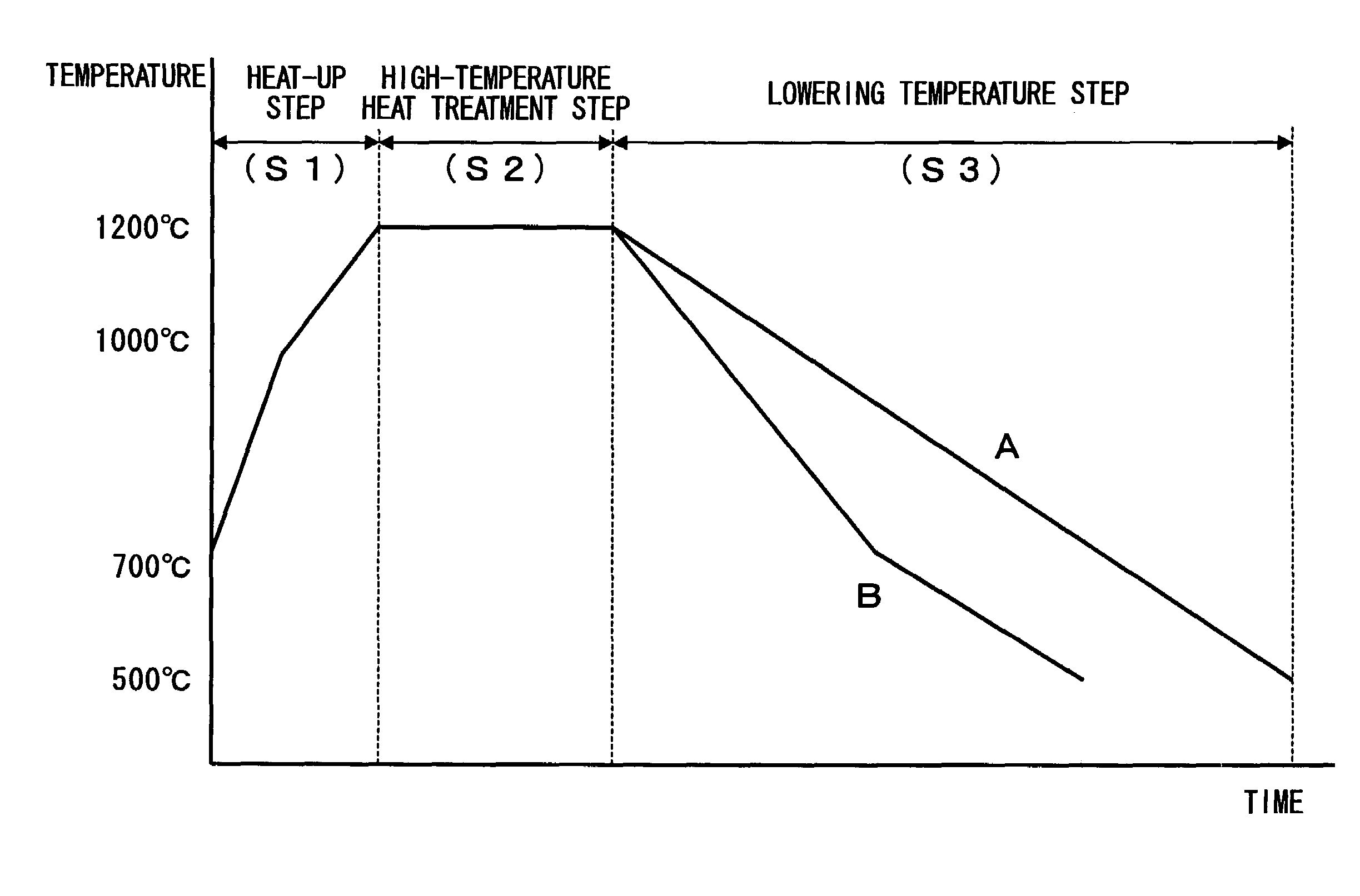
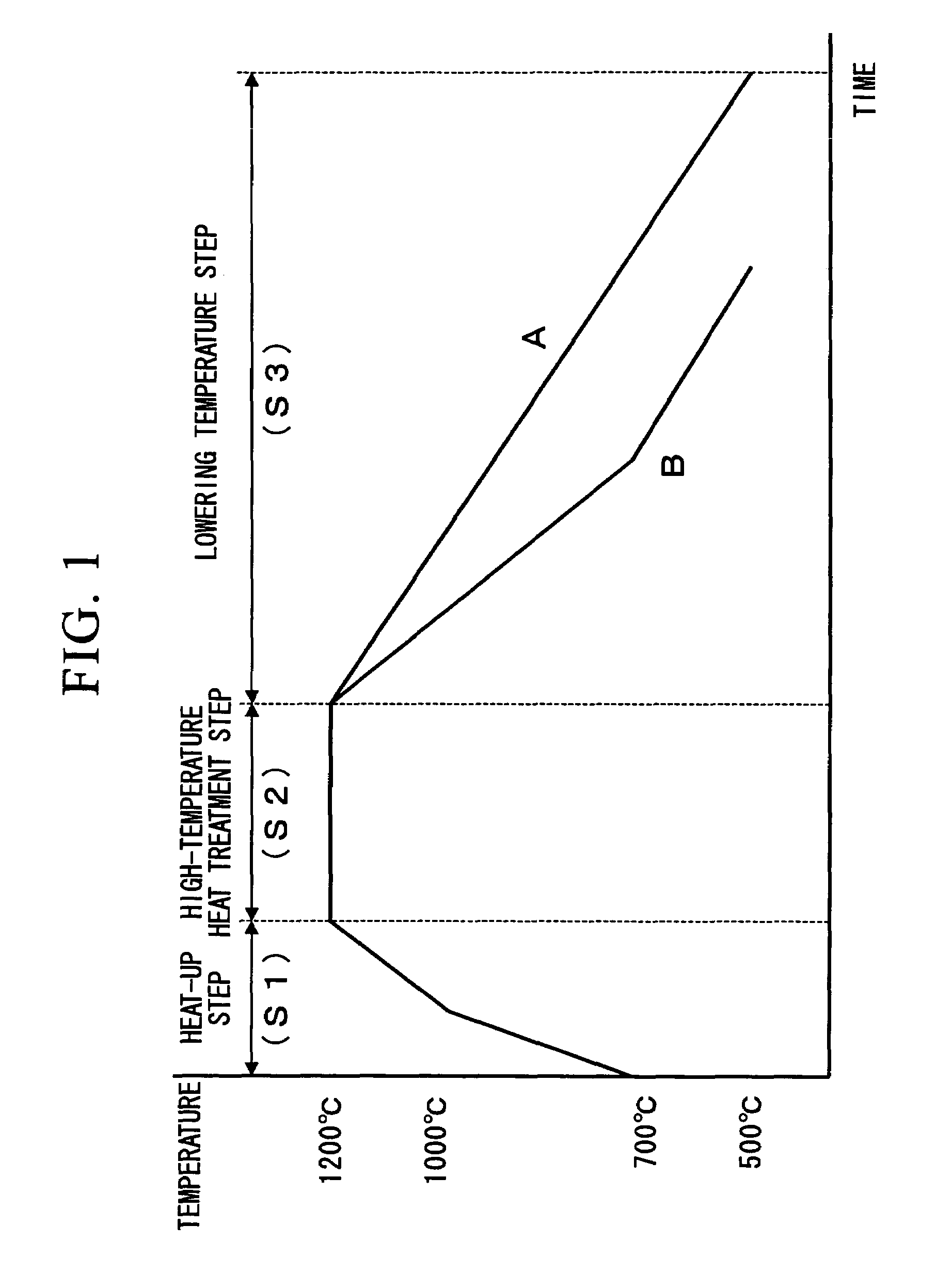
[0033]The method for heat-treating a silicon wafer of the present invention is illustrated in the following examples. Specifically, heat treatment experiments were carried out in which relationship between the ambient gas atmosphere and a lowering rate during lowering a temperature in the heat treatment of the silicon wafers was varied and iron concentration detected in the wafer surface was measured. Those heat treatment conditions and results obtained are described below.

[0034]The silicon wafers used in each experiment were all boron-doped p-type silicon wafers which had a diameter of 200 mm and a crystal plane orientation of (100) and had been cut from a single-crystal silicon ingot grown by the Czochralski (CZ) method, and mirror polished.

[0035]Common heat treatment conditions in the examples of the present invention and comparative examples were as follows. The above-described silicon wafers were loaded into a vertical thermal processing boat, and then the boat was placed in a ...


PUM

PropertyMeasurementUnit
temperatureaaaaaaaaaa

Abstract

This method for heat-treating a silicon wafer includes: a step of subjecting a silicon wafer to a high-temperature heat treatment in an ambient gas atmosphere of hydrogen gas, argon gas or a mixture thereof; and a step of lowering a temperature at a rate of 2° C. / min or less in a nitrogen-gas-containing ambient atmosphere in a portion or all of a process of lowering a temperature to a wafer removal temperature following said high-temperature heat treatment. This silicon wafer has a defect-free layer which is formed by a high-temperature heat treatment and is included in a surface thereof, wherein an average iron concentration in said surface is 1×10¹⁰ atoms / cm3 or less.

Description

CROSS REFERENCE TO RELATED APPLICATIONS[0001]This application is related to, but does not claim priority from, Japanese Patent Application No. 2004-032603, filed on Feb. 9, 2004, the contents of which are incorporated herein in their entirety by reference.BACKGROUND OF THE INVENTION[0002]1. Field of the Invention[0003]The present invention relates to a method for heat-treating silicon wafers and to silicon wafers.[0004]2. Background Art[0005]A surface layer portion of a silicon wafer sometimes contains oxygen precipitates and crystal defects having a regular octahedral structure known as crystal originated particles (COP) which are introduced into a crystal during pulling of a silicon single-crystal ingot. When present in the surface layer portion of the wafer where devices are fabricated, these defects cause a deterioration in the gate oxide integrity and other electrical characteristics.[0006]Therefore, in order to improve the gate oxide integrity and other electrical characterist...

Claims


Application Information

Patent Timeline
Patent Type & Authority Patents(United States)
IPC IPC(8): C30B25/12C30B25/14H01L21/324C30B29/06C30B33/02H01L21/322
CPCC30B33/02C30B29/06
Inventor KUSABA, TATSUMIOKUDA, HIDEHIKONONOGAKI, YOSHIHISA
Owner SUMCO CORP
Why Eureka
Try Eureka