
Chips, and apparatus and method for reaction analysis

a technology of reaction analysis and chips, applied in the field of reaction analysis, can solve the problem that patents cannot eliminate the possibility of air bubble mixing, and achieve the effects of high-speed reaction, easy control of minute amounts of fluid, and small internal volum

Active Publication Date: 2007-12-25
HITACHI LTD
View PDF10 Cites 8 Cited by
  • Summary
  • Abstract
  • Description
  • Claims
  • Application Information

AI Technical Summary

Benefits of technology

The present invention aims to provide chips with micro channels and an apparatus and method for chemical reactions that can solve the problems associated with microfluidic devices such as air bubbles, difficulty in removing air bubbles, complicated manufacturing processes, and limited shape options for the micro channels. The technical effects of the invention include improved control of minute amounts of fluid, high-speed reaction in a small space, and mass producibility of the devices.

Problems solved by technology

However, they also have problems due to their size (several microns to several hundred microns in width and depth).
In the above-mentioned two patents, consideration is given to the entrance of air bubbles into the channel, but the mechanisms disclosed in the above patents can not eliminate the possibility of mixing of air bubbles.

Method used


Image

  • Chips, and apparatus and method for reaction analysis
  • Chips, and apparatus and method for reaction analysis
  • Chips, and apparatus and method for reaction analysis

Examples


example 1

[0043]A reaction analyzer using the chips according to the present invention, particularly a biomolecule interaction analyzer, is explained here with reference to FIGS. 1 to 21 of the accompanying drawings. An exemplary process for analyzing the interaction between the biomolecules by using the biomolecule interaction analyzer according to the present invention is explained.

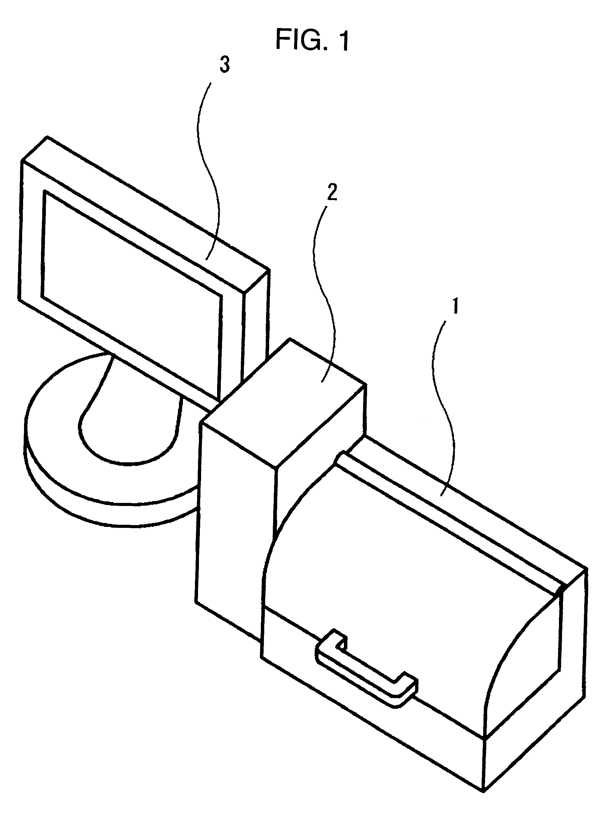
[0044]FIG. 1 is a bird's-eye view of the biomolecule interaction analyzer according to the present invention. This biomolecule interaction analyzer 1 is connected to a system unit 2 which controls the analyzer 1 and analyzes the signals detected by the analyzer. This system unit 2 is connected in turn to a monitor 3 which displays the contents of the work of the biomolecule interaction analyzer 1.

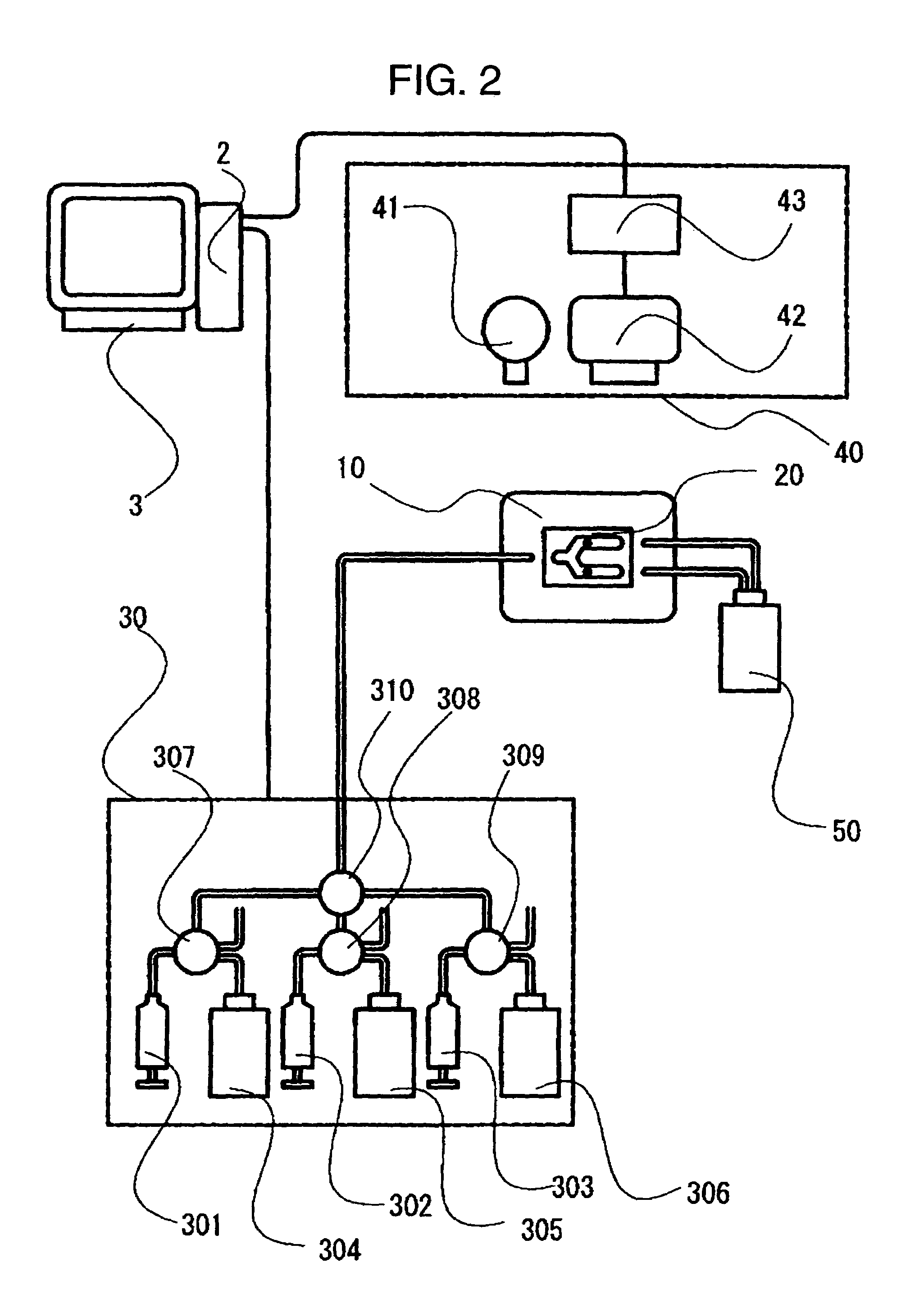
[0045]FIG. 2 is a general block diagram of the biomolecule interaction analyzer 1. Analyzer 1 comprises a chip 20 having fixated to the detecting region the probe molecules specifically bound to the objective biomolecule...

example 2

[0075]Shown here is an example of chip making use of surface plasmon resonance.

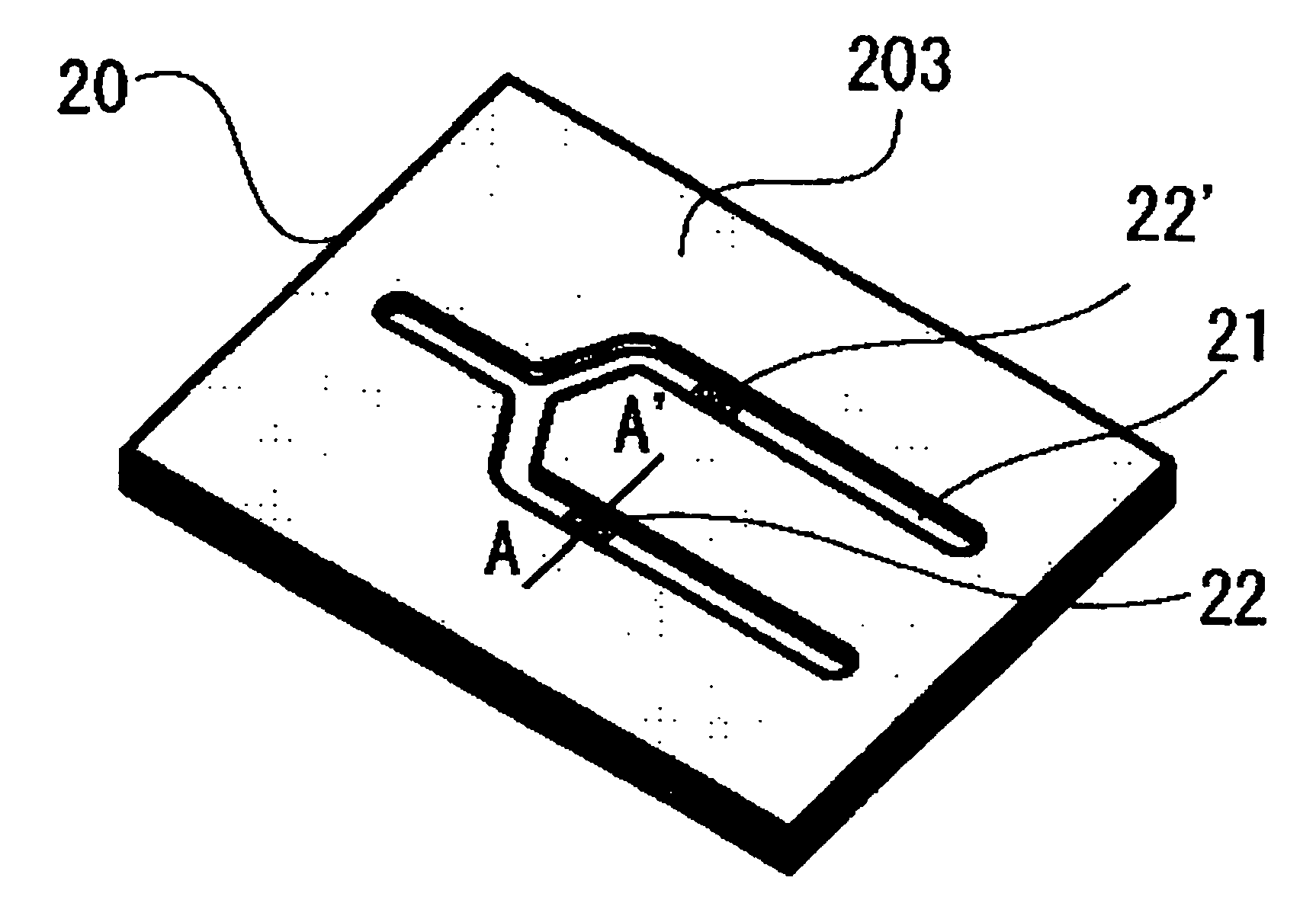
[0076]FIG. 18 is a bird's-eye view of chip 70. Chip 70 has a prism 704 on one side and a groove 71 on the other side, and detection regions 72, 72′ for detecting the objective biomolecules are provided on the surface of groove 71. In region 72, a probe for binding the objective biomolecules is provided, but no such probe is provided in region 72′ as in Example 1. The latter region 72′ is used as reference.

[0077]FIG. 19 is a cross section of chip 70. This chip 70 comprises a light-transmittable substrate 701, a metallic thin film layer 702, a water-repellant particle layer 703, a prism 704 and a detection region 72. There may be used, for instance, a quartz glass substrate as light-transmittable substrate 701, a thin film of gold as metallic thin film layer 702, and fine particles of a fluorine resin for water-repellant particle layer 703.

[0078]FIG. 20 is an exploded view of a combination of chip 70 and a ...


PUM

PropertyMeasurementUnit
sizeaaaaaaaaaa
refractive indexaaaaaaaaaa
widthaaaaaaaaaa

Abstract

A chip having a deaerating function and requiring no bonding or welding for forming a channel, and an apparatus and method for the reaction analysis are provided. The chip contains a first substrate, a second substrate having a liquid inlet and a liquid outlet, and an intermediate member having hydro-phobicity and air permeability and forming a channel between the first and second substrates. It is thereby possible to prevent mixing of air bubbles into the channel.

Description

INCORPORATION BY REFERENCE[0001]The present application claims priority from Japanese application JP2003-421957 filed on Dec. 19, 2003, the content of which is hereby incorporated by reference into this application.FIELD OF THE INVENTION[0002]The present invention relates to a reaction analysis relevant to a specific molecule in a specimen and a chip used therefor.BACKGROUND OF THE INVENTION[0003]With the substantial completion of decoding the human genome in 2001 as a turning point, the focus of studies in the field of biotechnology research is shifting from genomic to proteomic research in which pursuit is made about when, where and how genetic information possessed by individual living things is expressed in making proteins, and how these produced proteins function in the cells of individual organisms in cooperation with other proteins. The function of most proteins is related to their interaction with other biomolecules, so that one of the momentous subjects in the study of prot...

Claims


Application Information

Patent Timeline
Patent Type & Authority Patents(United States)
IPC IPC(8): B32B27/04B32B27/06B32B27/08B32B27/14G01N21/03B01L3/00C12M1/00C12N15/09C12Q1/68G01N35/08G01N37/00H01L21/31H01L23/58
CPCB01L3/502723B01L3/502707B01L2200/0684B01L2300/0654B01L2400/0415B01L2300/0864B01L2300/165B01L2400/0406B01L2300/0816
Inventor TAKENAKA, KEIFUJIMURA, TORUGOTO, YASUSHI
Owner HITACHI LTD
Learn More