Method for manufacturing a solid-state image sensing device, such as a CCD

a solid-state image and sensing device technology, applied in the direction of color television, television system, radio control device, etc., can solve the problems of color reproduction difficulty and add to the increase of assembly man-hours

Active Publication Date: 2008-01-08
SEMICON COMPONENTS IND LLC
View PDF15 Cites 14 Cited by
  • Summary
  • Abstract
  • Description
  • Claims
  • Application Information

AI Technical Summary

Benefits of technology

[0006]For the reason described above, in conventional solid-state image sensing devices, an infrared cut-off filter is attached to the surface of the package, which adds to the increase in assembly man-hours. The present invention has been made to solve the above shortcoming, and has as its object to provide a method for manufacturing a solid-state image sensing device fitted with an infrared cut-off filter without increasing the assembling man-hours.

Problems solved by technology

This is conspicuous in the light rays from heat sources, such as the light of an electric bulb, which makes color reproduction difficult.
For the reason described above, in conventional solid-state image sensing devices, an infrared cut-off filter is attached to the surface of the package, which adds to the increase in assembly man-hours.

Method used


Image

  • Method for manufacturing a solid-state image sensing device, such as a CCD
  • Method for manufacturing a solid-state image sensing device, such as a CCD
  • Method for manufacturing a solid-state image sensing device, such as a CCD

Examples


Embodiment Construction

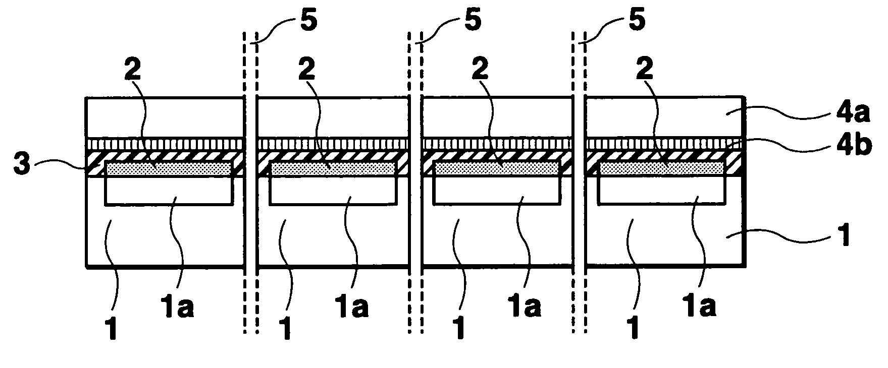
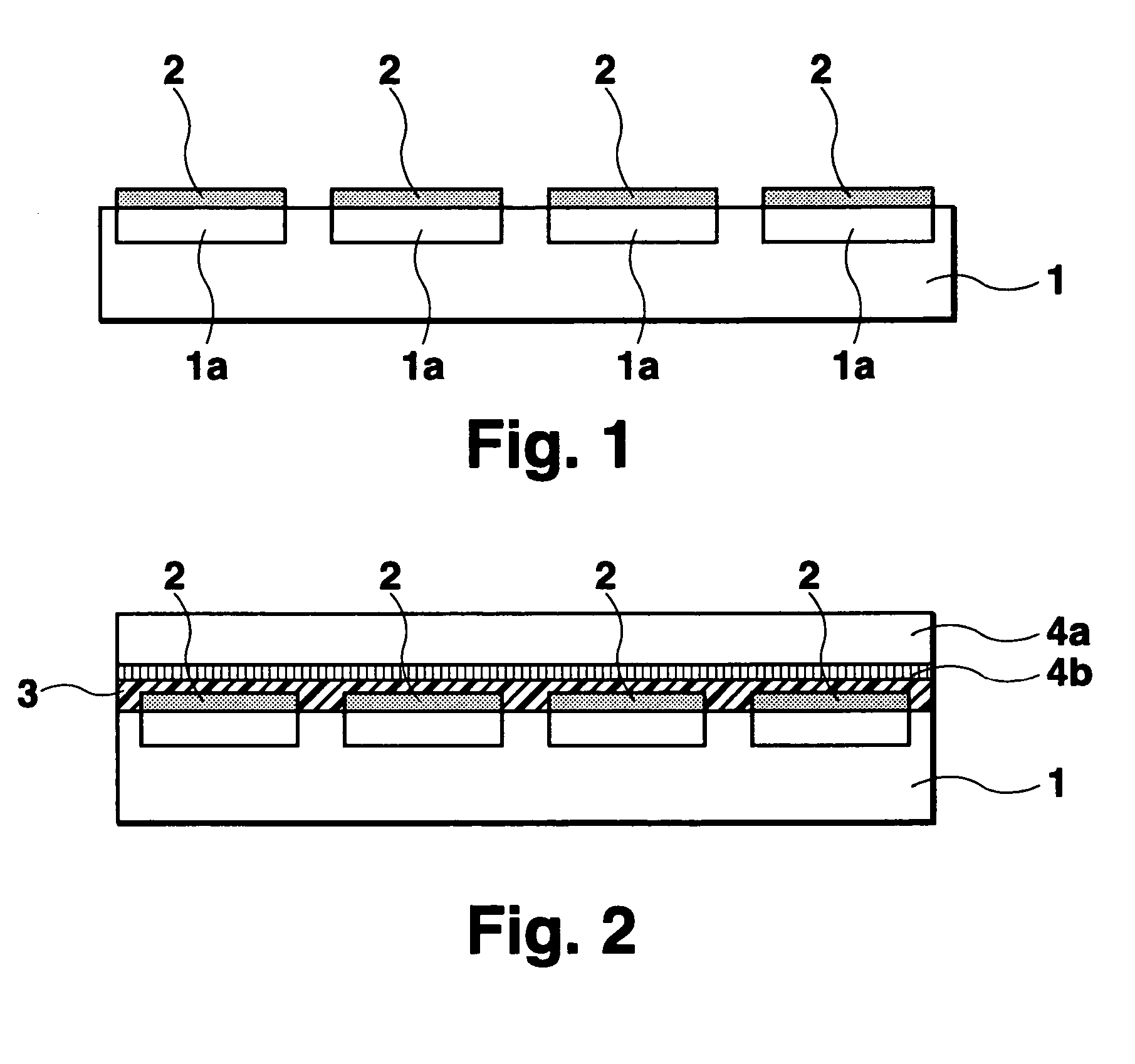
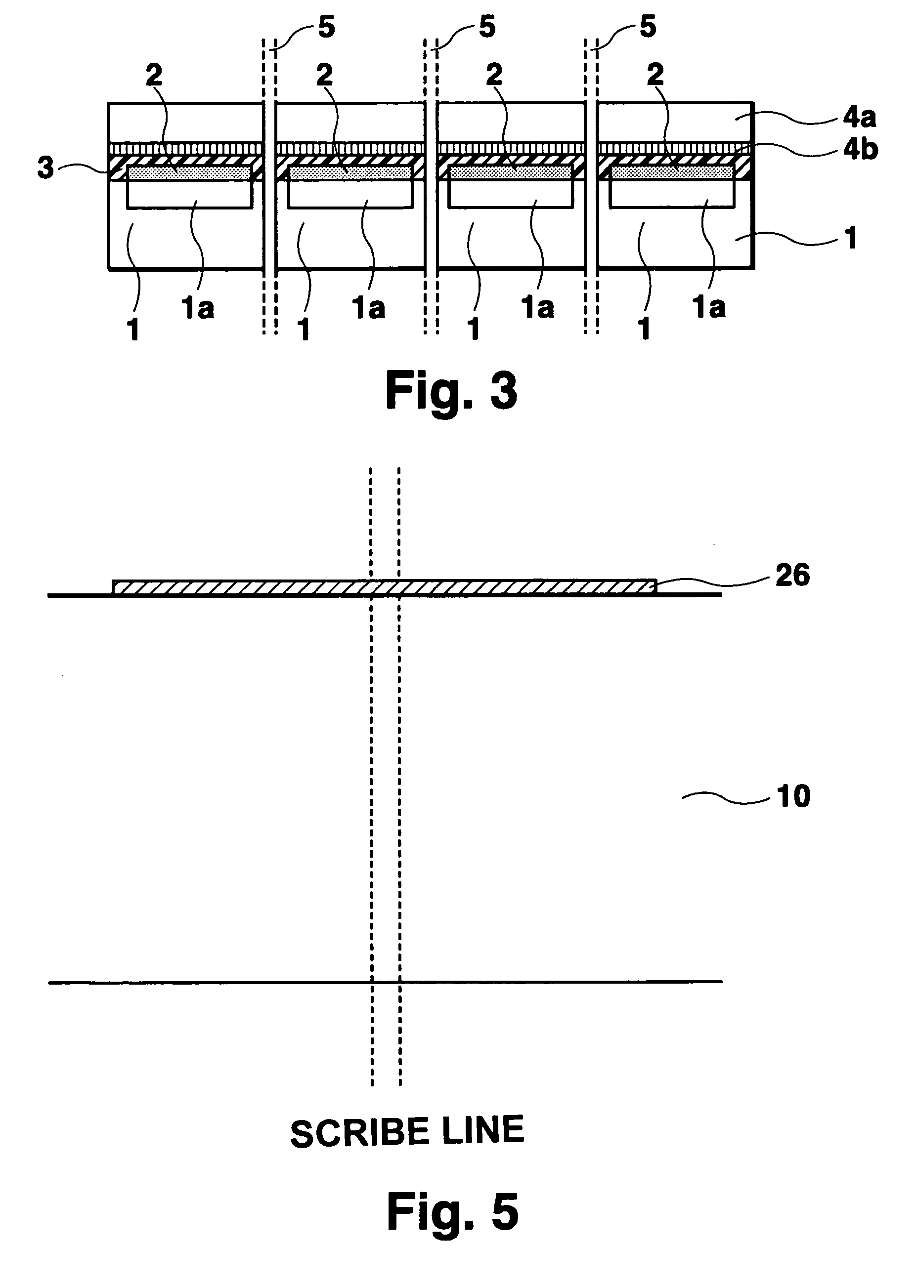
[0022]FIGS. 1 to 3 are sectional views in the order of processes showing a first embodiment in a process for manufacturing a solid-state image sensing device of the present invention. The method of this embodiment comprises a process of forming a light detecting element, a process of depositing layers to form an infrared cut-off filter, and a dicing process as shown in the flowchart in FIG. 4.

[0023]In the process of forming a light detecting element in Step S10, as shown FIG. 1, light detecting elements are formed in respective areas la which are marked off by scribe lines on the surface of a semiconductor substrate 1. The color filters 2 are deposited over the areas 1a where the light detecting elements have been formed. The semiconductor substrate 1 may be formed of an ordinary semiconductor material, such as silicon, gallium arsenide, for example. An integrated circuit, such as a CCD as a light detecting device, can be formed by a well-known semiconductor process.

[0024]In the pro...


PUM


Abstract

Light detecting elements are formed in areas marked off by scribe lines on a semiconductor substrate, and color filters are deposited in such a manner as to cover the formed areas of the light detecting elements, and then an infrared cut-off filter, on which an infrared reflecting film is vapor-deposited in such a manner as to cover the formed areas of the light detecting elements, is firmly fixed to the surface of the semiconductor substrate through the interposition of a translucent resin layer, such as an epoxy adhesive, to thereby form a multilayered structure, and this multilayered structure is diced along scribe lines.

Description

CROSS REFERENCE TO RELATED APPLICATION[0001]The priority application Number JP2003-187695 upon which this patent application is based is hereby incorporated by reference.BACKGROUND OF THE INVENTION[0002]1. Field of the Invention[0003]The present invention relates to a method for manufacturing a solid-state image sensing device, such as a CCD.[0004]2. Description of the Related Art[0005]An infrared cut-off filter for removing infrared components from incident light is indispensable in color solid-state image sensing devices, which are commonly used in TV cameras and digital still cameras. Without this infrared cut-off filter, because infrared light is contained in the incident light, the solid-state image sensing device is sensitive to infrared light, and therefore the output of the solid-stage image sensing device includes not only visible light components but also error components from the infrared light. This is conspicuous in the light rays from heat sources, such as the light of...

Claims


Application Information

Patent Timeline
Patent Type & Authority Patents(United States)
IPC IPC(8): H01L21/00H01L27/14H01L27/146H01L27/148H01L31/00H01L31/09H04N5/335H04N5/357H04N5/369H04N5/372
CPCH01L27/1462H01L31/02162H01L27/14621H01L27/14636H01L27/14685H01L27/14687H01L27/14831
Inventor KOJIMA, KAZUAKIHAMADA, MINORU
Owner SEMICON COMPONENTS IND LLC
Why Eureka
Try Eureka