Display panel and display panel driving method

a technology of display panel and driving method, which is applied in the field of display panel, can solve the problems of not being able to achieve accurate tone control, unable to display images with a desired luminance tone for long time periods, and it is difficult to make the characteristics of transistors 104/b> of individual pixels uniform, etc., to suppress the influence of voltage-current characteristic variations, display stable effect, and display area per pixel of display panel

Active Publication Date: 2008-01-08
SOLAS OLED LTD
View PDF64 Cites 88 Cited by
  • Summary
  • Abstract
  • Description
  • Claims
  • Application Information

AI Technical Summary

Benefits of technology

[0012]Accordingly, one advantage of the present invention is that pixels stably display images with desired luminance in a display panel.
[0013]Another advantage of the present invention is that the display area per pixel of a display panel is increased.DISCLOSURE OF INVENTION
[0014]To achieve the above advantages, a display panel according to one aspect of the present invention comprises:
[0015]one or more optical elements which have a pair of electrodes and exhibit an optical operation corresponding to an electric current flowing between the pair of electrodes;
[0017]one or more switch circuits which supply a memory current having a predetermined current value to the current line during a selection period, and stop supply of a current to the current line during a non-selection period; and
[0018]one or more current memory circuits which store current data corresponding to the current value of the memory current flowing through the current line during the selection period and, in accordance with the current data stored during the selection period, supply a display current having a current value substantially equal to the memory current to the optical element during the non-selection period.

Problems solved by technology

Therefore, it is difficult to display images with a desired luminance tone for long time periods.
As a consequence, no accurate tone control can be performed.
However, as the resolution of an EL element increases, it becomes more difficult to make the characteristics of the transistors 104 of the individual pixels uniform.
When an amorphous silicon transistor is used, however, good physical properties with which the transistor functions well cannot be obtained.
This makes it impossible to apply amorphous silicon transistors which can be fabricated at a relatively low cost.
However, when a large number of transistors are formed, the emission area of one pixel decreases.
Unfortunately, this shortens the light emission life because the organic EL layer is applied with a higher voltage and current.
As a consequence, the power consumption is high.

Method used


Image

  • Display panel and display panel driving method
  • Display panel and display panel driving method
  • Display panel and display panel driving method

Examples


first embodiment

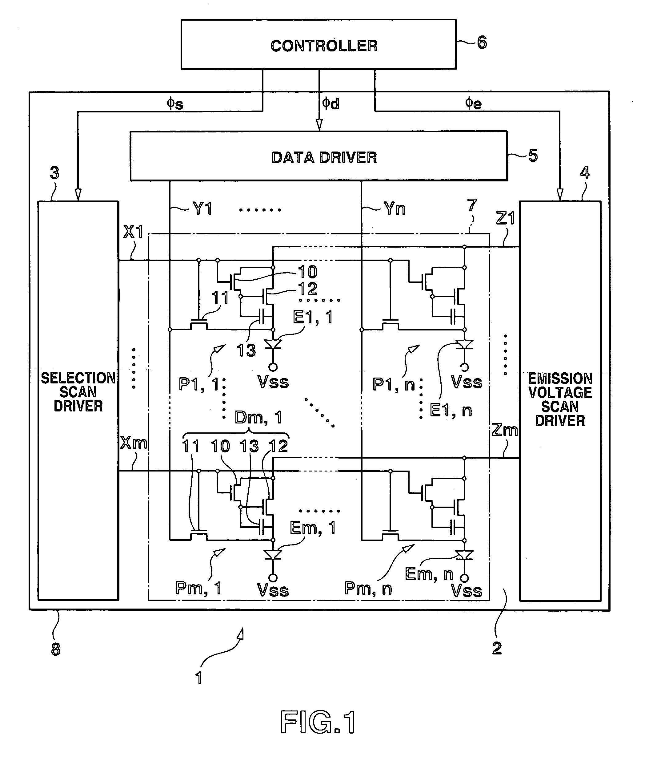
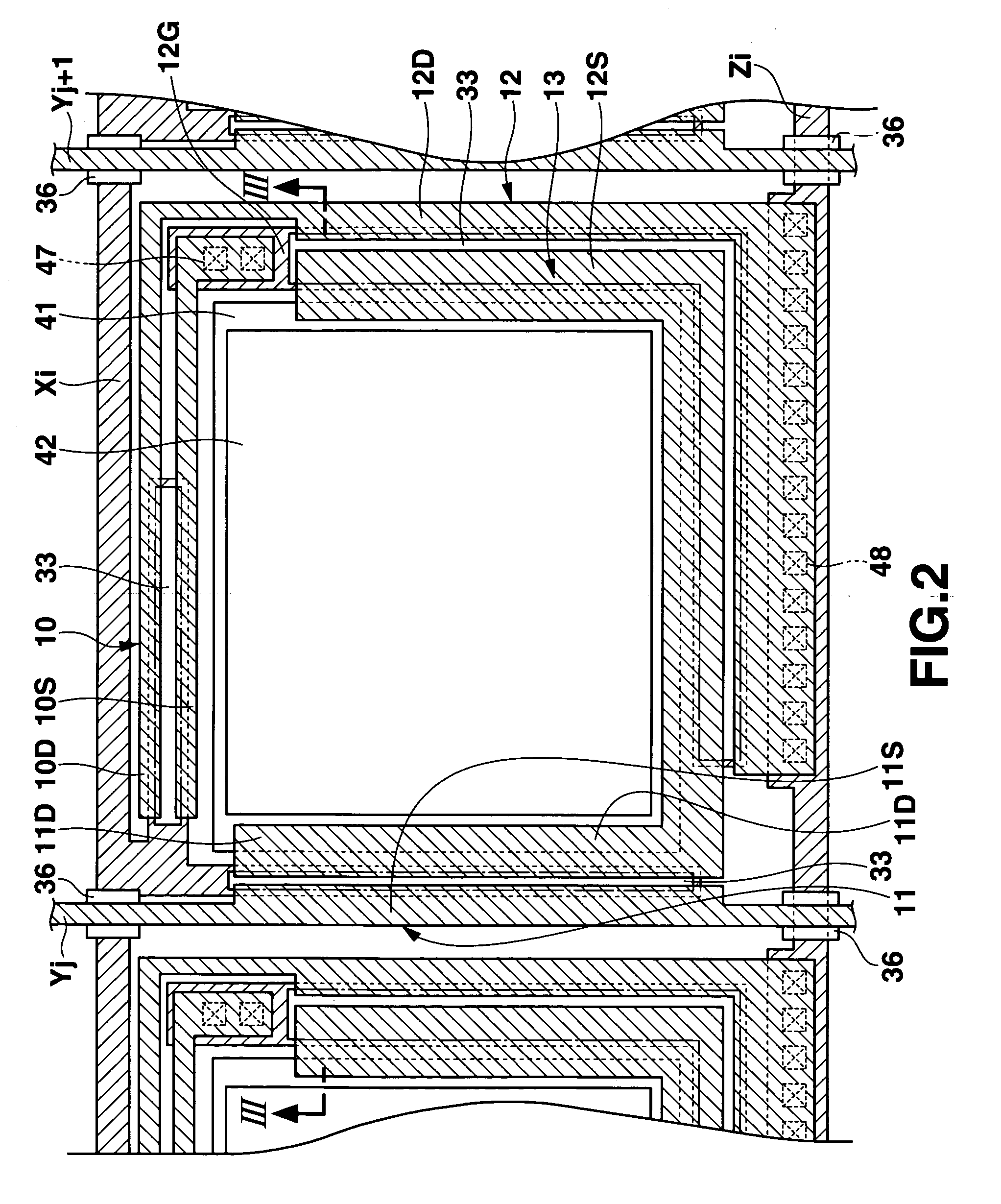
[0041]FIG. 1 is a block diagram showing a practical arrangement of a light emitting element display to which the present invention is applied. As shown in FIG. 1, the light emitting element display 1 includes, as its basic configuration, an active matrix type light emitting panel (driver) 2 and a controller 6 for controlling the whole light emitting display 1. The light emitting element display 1 is a so-called active matrix driving type display device. The light emitting panel 2 includes a transparent substrate 30 (shown in FIG. 3) which is made of, e.g., borosilicate glass, silica glass, and another glass which is resistant against temperatures during a transistor fabrication process (to be described later). Light emitting unit 7 is formed on the transparent substrate 30, has a plurality of pixels and emits light so as to display an image corresponding to image data from the controller 6. A selection scan driver 3, emission voltage scan driver 4, and data driver 5 are formed on th...

second embodiment

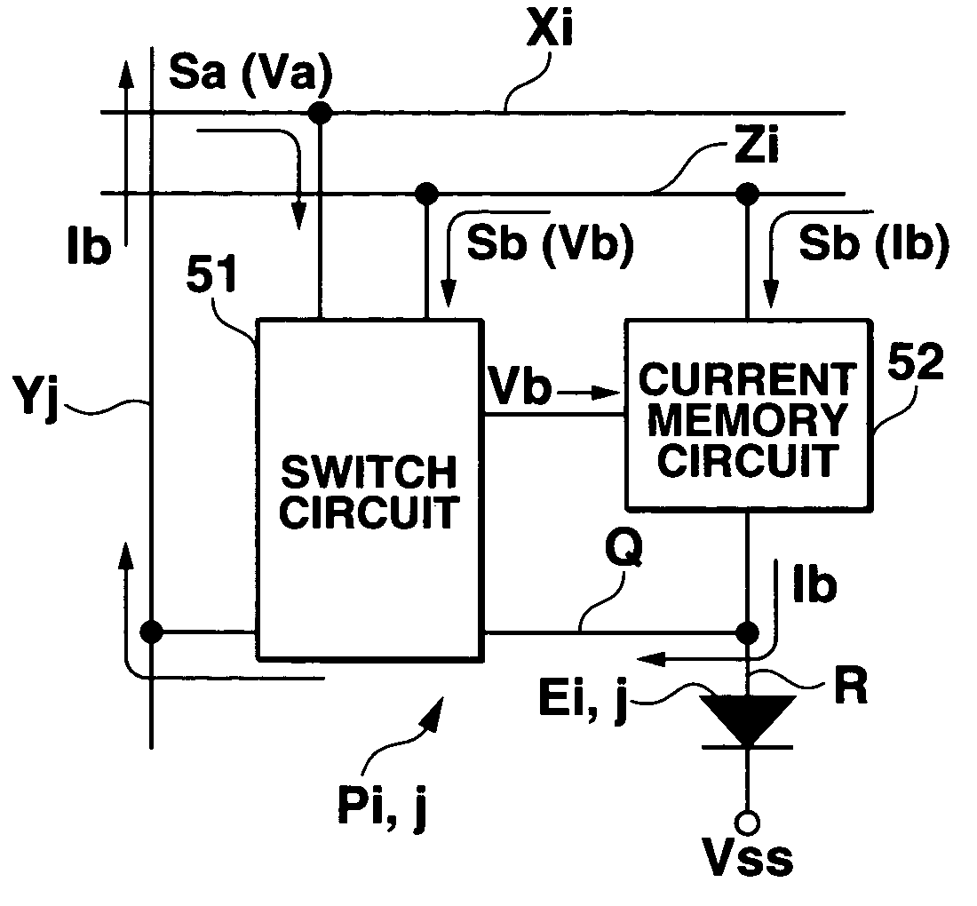
[0095]The second embodiment will be described next. This second embodiment is the same as the first embodiment except for the arrangement of each pixel Pi,j. That is, in this second embodiment as shown in FIGS. 8A and 8B, each pixel Pi,j (a pixel driving circuit Di,j of each pixel Pi,j) has a switch circuit 51 instead of transistors 10 and 11, and a current memory circuit 52 instead of a transistor 12 and capacitor 13. The same reference numerals as in the above first embodiment denote the same parts, so a detailed explanation thereof will be omitted.

[0096]A power supply signal Sb output to an emission voltage scan line Zi has a voltage value Vb during a selection period TSE and a voltage value Vb′ during a non-selection period TNSE. These voltage values Vb and Vb′ correspond to the non-selection voltage VNSE and reference voltage VSS, respectively, shown in FIG. 7.

[0097]A scan signal Sa output to a selection scan line Xi has a voltage value Va which turns on the switch circuit 51 d...

third embodiment

[0100]The third embodiment will be described below. This third embodiment is the same as the first embodiment except for the arrangement of each pixel Pi,j. That is, as shown in FIGS. 9A and 9B, each pixel Pi,j of the third embodiment has a transistor 14 instead of a transistor 10. The same reference numerals as in the above first embodiment denote the same parts, so a detailed explanation thereof will be omitted.

[0101]Unlike the transistor 10, a drain electrode 14D and gate electrode 14G of the transistor 14 are connected to a selection scan line Xi, and a source electrode 14S of this transistor 14 is connected to a gate electrode 12S of a transistor 12. Similar to a transistor 11 and the transistor 12, the transistor 14 is an n-channel amorphous silicon thin film transistor.

[0102]This transistor 14 operates by the application of a voltage such as that shown in the waveform chart shown in FIG. 7. During a selection period TSE, the transistor 14 is turned on by an ON-level (high-lev...


PUM


Abstract

A display panel includes an optical element which has a pair of electrodes and exhibits an optical operation corresponding to an electric current flowing between the electrodes, and a switch circuit which supplies a memory current having a predetermined current value to a current line during a selection period, and stops the supply of the memory current to the current line during a non-selection period. A current memory circuit stores current data corresponding to the current value of the memory current flowing through the current line during the selection period and, in accordance with the current data stored during the selection period, supplies a display current having a current value substantially equal to the memory current to the optical element during the non-selection period.

Description

[0001]This application is a U.S. National Phase Application under 35 USC 371 of International Application PCT / JP02 / 13034 filed Dec. 12, 2002.TECHNICAL FIELD[0002]The present invention relates to a display panel having an active driving type optical element and a method of driving the same, and to a driving circuit and the like of, e.g., a light emitting element as the optical element.BACKGROUND ART[0003]A light emitting element display is conventionally known in which light emitting elements such as organic EL (electroluminescent) elements, inorganic EL elements, or light emitting diodes are arrayed in a matrix manner as optical elements, and the respective light emitting elements emit light to display an image. In particular, an active matrix driving type light emitting element display has advantages such as high luminance, high contrast, high resolution, and low power consumption. Therefore, such displays are developed in recent years, and particularly an organic EL element has at...

Claims


Application Information

Patent Timeline
Patent Type & Authority Patents(United States)
IPC IPC(8): G09G3/12H01L51/50G09G3/20G09G3/30G09G3/32H01L27/32
CPCG09G3/325G09G2300/0417H01L27/3244G09G2300/0842G09G2300/0866G09G2300/0439H10K59/12G09G3/30
Inventor SHIRASAKI, TOMOYUKIYAMADA, HIROYASUHATTORI
Owner SOLAS OLED LTD
Why Eureka
Try Eureka