Display module

a display module and active matrix technology, applied in the field of can solve the problems of difficult application of terminal configuration to active matrix type display modules, and achieve the effect of narrowing the area of effective display regions and high quality

Inactive Publication Date: 2005-09-20
SAMSUNG DISPLAY CO LTD +1
View PDF7 Cites 37 Cited by
  • Summary
  • Abstract
  • Description
  • Claims
  • Application Information

AI Technical Summary

Benefits of technology

[0057]By using the above configuration of (1) to (8), a high quality display module is obtained preventing a data signal that is written anew from being affected by the previous signal data and a display module that will not narrow the area of an effective display region can be provided.

Problems solved by technology

However, it is difficult that such terminal configuration is applied to an active matrix type display module as is.

Method used


Image

  • Display module
  • Display module
  • Display module

Examples


first embodiment

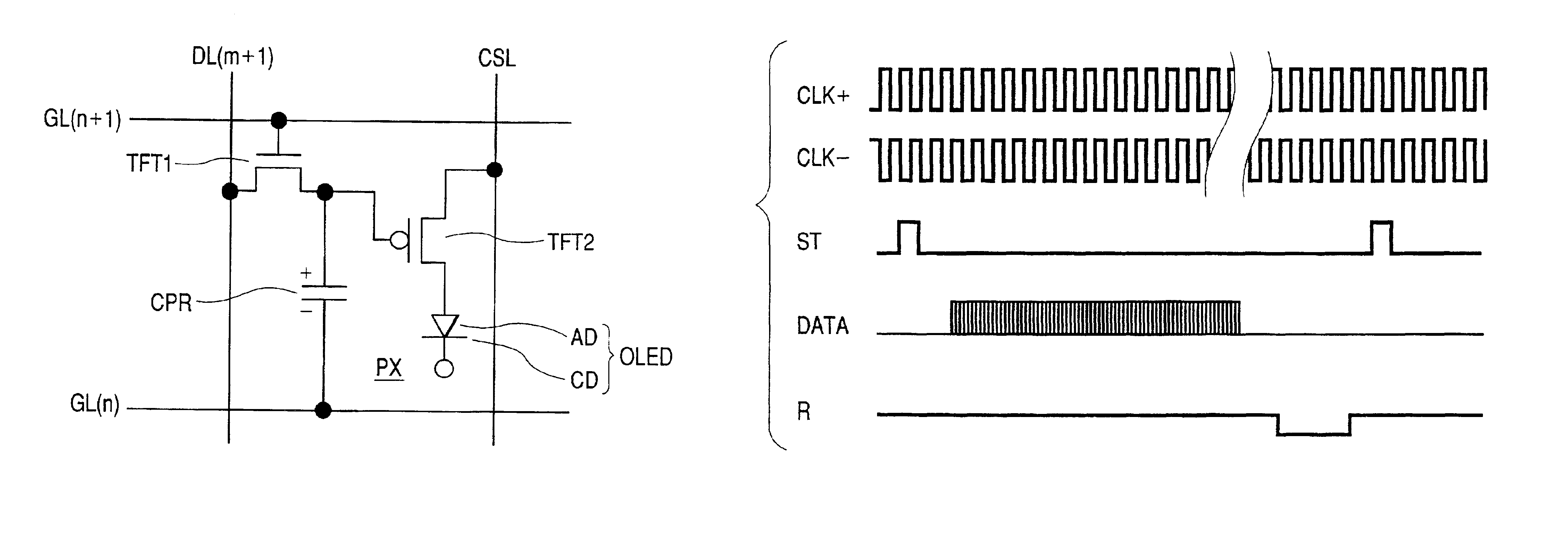
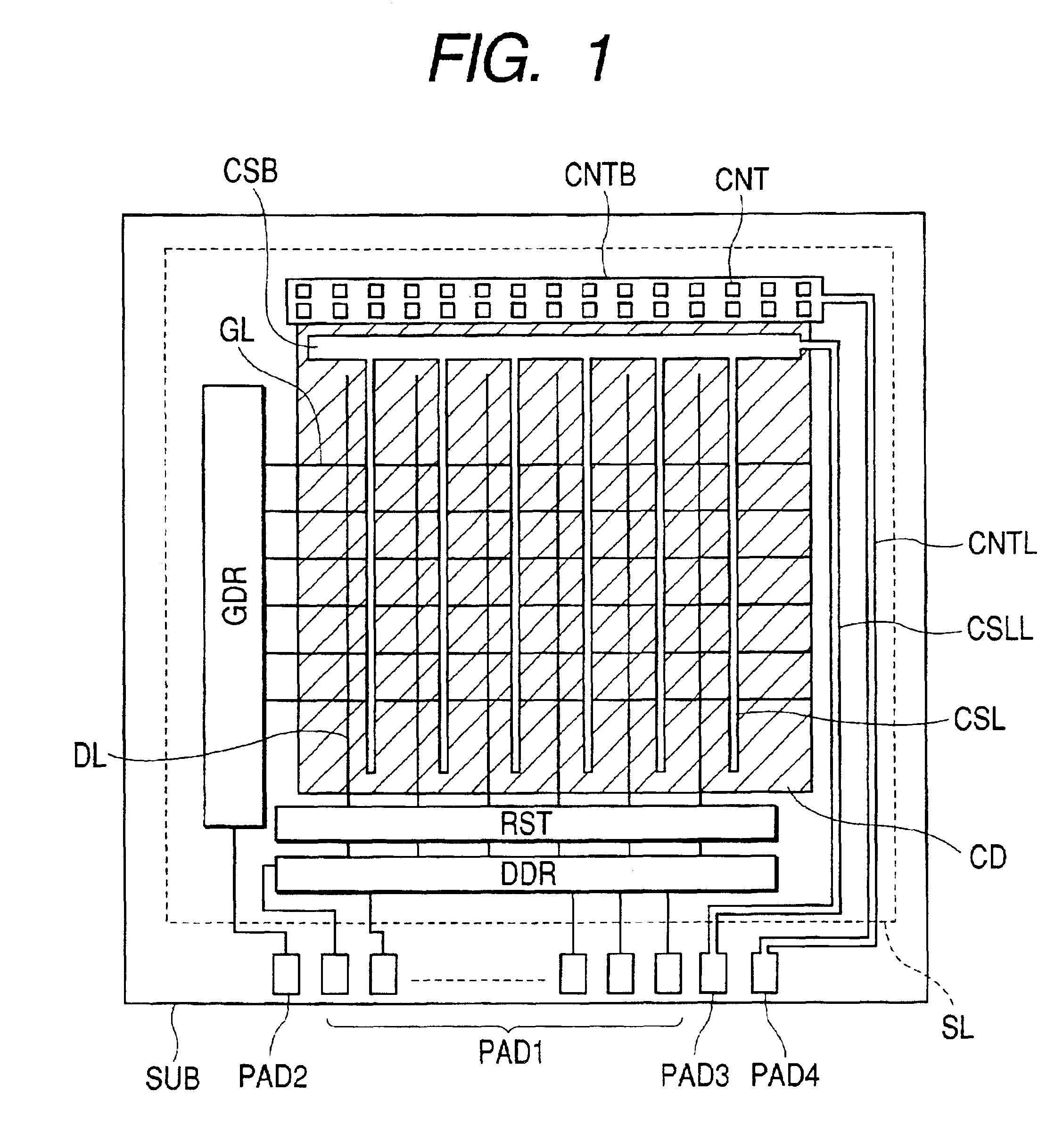
[0086]FIG. 3 is a block diagram for describing the principal part of the configuration of the display module according to the present invention. Many pixels of the configuration described in FIG. 2 described above are arranged in a matrix shape in a display region AR. The part of a data driving circuit and only a data line are shown here.

[0087]Further, FIG. 4 is a timing drawing for describing the operation of the embodiment of FIG. 3. Each signal shown using the same reference symbol In FIGS. 3 and 4 is identical. The configuration and operation of FIG. 3 are described below with reference to the timing chart of FIG. 3.

[0088]A data driving circuit DDR shows a shift register SR and a sampling circuit SAP and the detailed configuration is not illustrated. The data driving circuit is provided with the 1-system shift register SR that inputs a start pulse ST and pixel clock signals (hereinafter simply referred to as clocks) CLK+ and CLK− and sequentially transfers a data signal DATA to ...

second embodiment

[0100]FIG. 5 is a block diagram for describing the principal part of the configuration of the display module according to the present invention. Many pixels of the configuration described in FIG. 2 are arranged in a matrix shape in a display region AR in the same manner as FIG. 3. Further, FIG. 5 also shows the part of a data driving circuit and only a data line.

[0101]This embodiment differs from the first embodiment in that a reset circuit RST is arranged at the opposite side (termination position of a data line DL) with a display region AR sandwiched for a data driving circuit DDR. The circuit configuration of the shift register SR, the sampling circuit SAP, and the reset circuit RST and the timing are identical with those of the first embodiment.

[0102]In this embodiment, the effect of noises resulting from various wiring layouts on a substrate can be reduced because a reset circuit RST is provided at a distant position from a data driving circuit DDR. Further, when a reset circui...


PUM


Abstract

This display module performs a high quality display by preventing the effect resulting from a residual charge of a data signal in the previous scanning remaining in a capacitor of a pixel circuit.
The display module is provided with the pixel circuit having an active element that selects a pixel by a horizontal scanning signal supplied from a scanning line GL every intersection unit of multiple scanning lines GLs arranged in a matrix within a display region AR on a substrate SUB, a data holding element that holds a data signal supplied from the data line by the turn-on of this active element, and an organic light emitting diode OLED that emits light by the current supplied from a current supply line CSL in accordance with the data signal held in the data holding element, and a reset circuit RST that recovers at least either a capacitor CPR or a data line DL of the pixel circuit to an initial condition is provided before data for the pixel that corresponds to the next scanning line is sent to the data line after the scanning of the scanning line before one is finished.

Description

FIELD OF THE INVENTION[0001]The present invention relates to an active matrix type display module, and more particularly to a display module provided with a pixel composed of an emitting device, such as an electro luminescence element or an LED (light emitting diode) that emits light by applying electric current to an emitting layer, such as an organic semiconductor thin film and a pixel circuit that controls the light emission operation of this pixel.BACKGROUND OF THE INVENTION[0002]In recent years, with the advent of advanced information society, the demand of a personal computer, a car navigation system, a portable terminal unit, a telecommunications system or these combined products is increasing. A thin, lightweight, and low power consumption display device is suitable for a display means of these products and a liquid crystal display module or a display module that uses an electrooptic element, such as a self light emission type EL element or an LED is used.[0003]The display m...

Claims


Application Information

Patent Timeline
Patent Type & Authority Patents(United States)
IPC IPC(8): G09G3/32G09F9/30H01L51/50G09G3/20G09G3/30
CPCG09G3/3233G09G3/3291G09G2300/0842G09G2300/0876G09G2310/0248G09G2310/0251G09G2310/0262G09F9/30
Inventor SATO, TOSHIHIROKANEKO, YOSHIYUKIMIKAMI, YOSHIROOUCHI, TAKAYUKI
Owner SAMSUNG DISPLAY CO LTD
Why Eureka
Try Eureka