Drive circuit of display apparatus

a drive circuit and display device technology, applied in the direction of instruments, television systems, static indicating devices, etc., can solve the problems of large scale of the drive circuit and inability to provide a method for determining image data stored in line memory all, so as to reduce the power consumption of the drive circuit

Active Publication Date: 2008-01-08
RENESAS ELECTRONICS CORP
View PDF8 Cites 9 Cited by
  • Summary
  • Abstract
  • Description
  • Claims
  • Application Information

AI Technical Summary

Benefits of technology

[0014]Therefore, an object of the present invention is to provide a drive circuit of a d

Problems solved by technology

Therefore, a new problem arises in that the scale of drive circuit becomes large.
However, the conventio

Method used


Image

  • Drive circuit of display apparatus
  • Drive circuit of display apparatus
  • Drive circuit of display apparatus

Examples


first embodiment

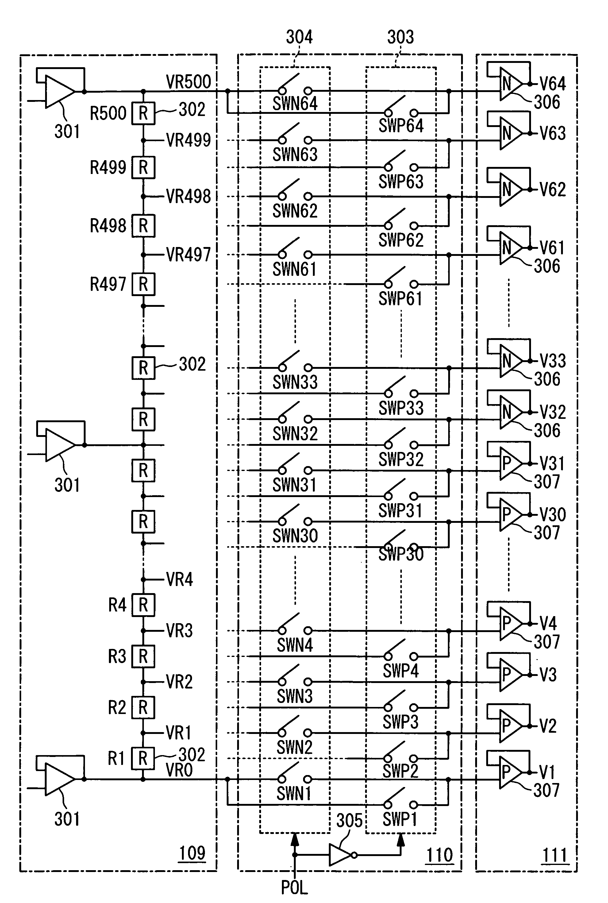
[0060]FIG. 4 is a block diagram showing the configuration of a display apparatus, e.g., a liquid crystal display device to which the present invention is applied. A display apparatus 1000 used for a portable phone, etc. is connected to a CPU 2, and displays an image in response to a signal 12 from the CPU 2. Though not shown in the figure, the display apparatus 1000 includes a display unit having a plurality of scanning lines and a plurality of data lines arranged in a matrix of rows and columns. The display apparatus 1000 contains a data line drive circuit 1, an interface circuit 3, a RAM control circuit 4, a command control circuit 5, a timing control circuit 6, a scanning line drive circuit 7, an oscillation circuit 8 a timing generating circuit 9, a power supply circuit 10, and a Vcom circuit 11.

[0061]The data line drive circuit 1 drives the data lines of the display unit and contains a later-described frame memory 101 and a data determination circuit 107. The interface circuit ...

second embodiment

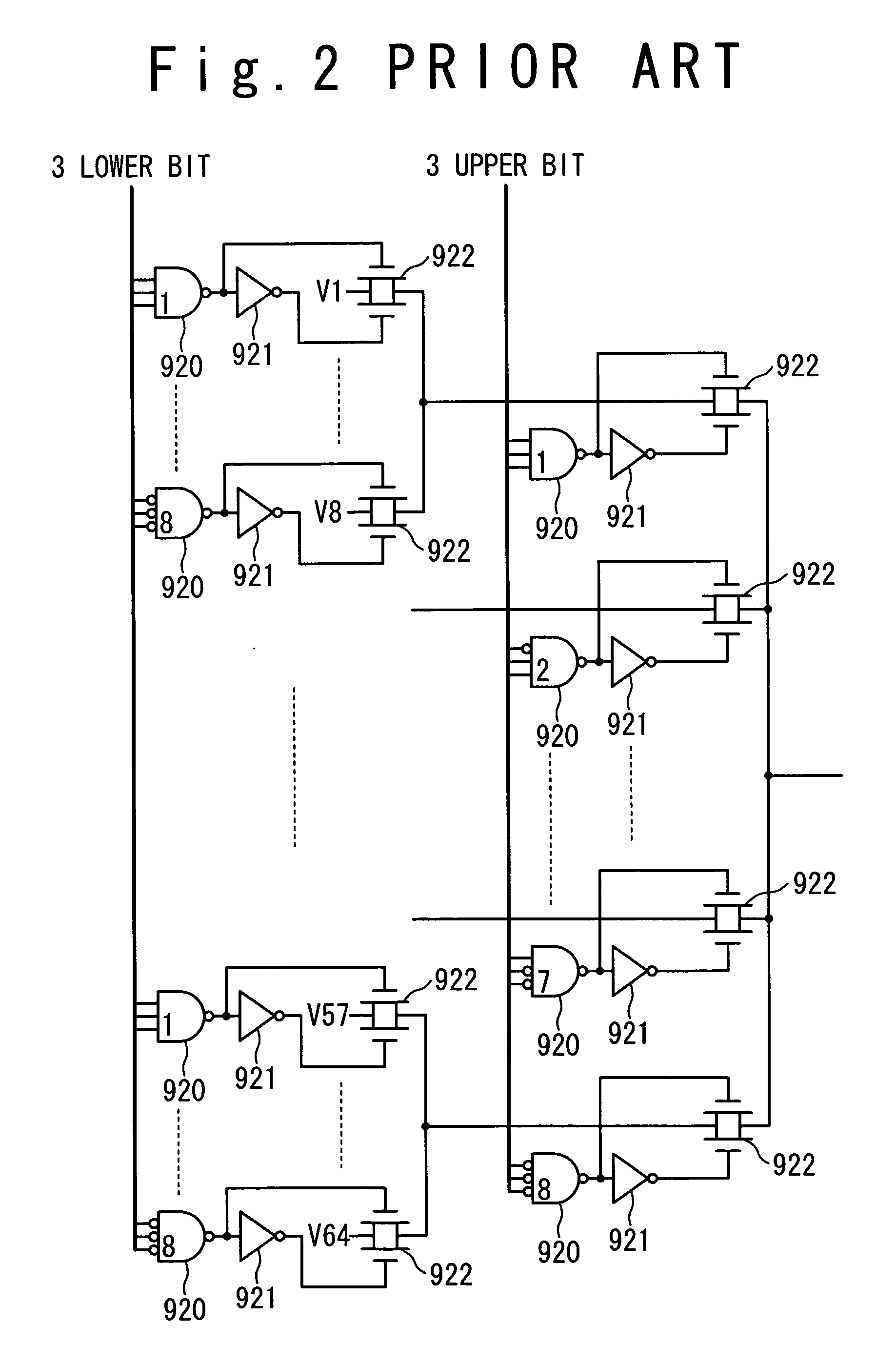
[0082]FIG. 15 is a block diagram of the data line drive circuit 1 according to the second embodiment of the present invention, and FIG. 16 shows the circuit configuration which contains the data determination circuit 107 for the data determination. The second embodiment is different from the first embodiment in a part of the circuit structure. In the first embodiment, the switches 206 which are connected to the data lines are set to the off state, and any voltage is not applied to the data lines in the case of the data determination. However, in the second embodiment, the voltage of GND or VDD is applied in the case of the data determination. For this purpose, as shown in FIG. 16, the switches 203a which are connected to the gradation lines 204 and the switches 207a which are connected to the outputs of the gradation selection switches 205 are common between the first and second embodiments. Also, switches 203b which are connected to the gradation lines 204 and switches 207b which a...

third embodiment

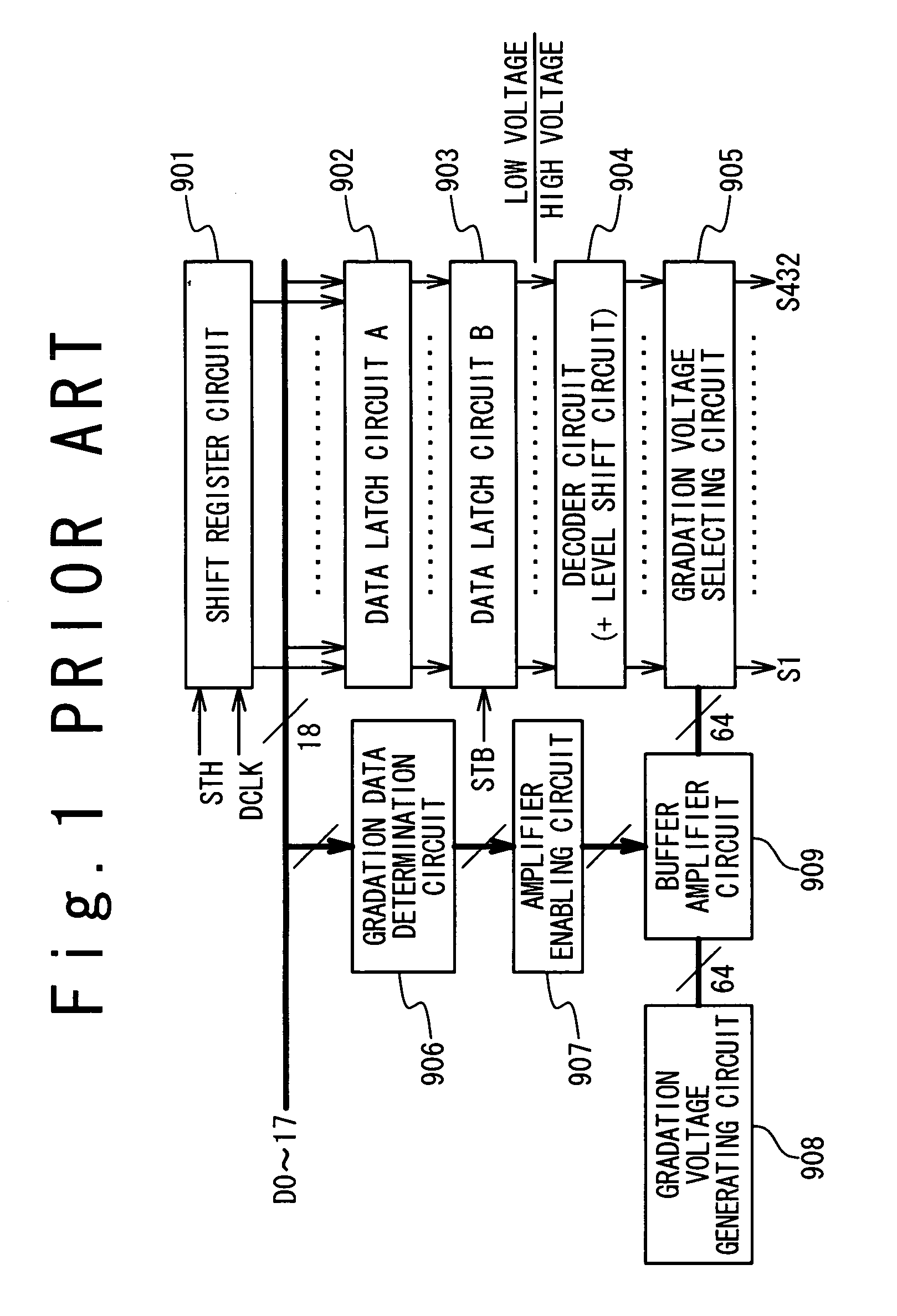
[0090]FIG. 19 shows a block diagram of the data line drive circuit 1 according to the third embodiment of the present invention. In this embodiment, the position of a shift register circuit A 601 is different, compared with the conventional structure shown in FIG. 1 In the conventional example, the shift register circuit 901 is provided in the front-stage of the data latch circuit A 902 and has the function to generate the sampling signal such that the image data is latched in the data latch circuit A 902 in order. However, in this embodiment, the shift register circuit 601 is provided in the back-stage of the data latch circuit A 102, and has the function to transfer the image data latched in the data latch circuit A 102 to the data determination circuit 107 in order in synchronous with a clock signal RCLK.

[0091]Also, FIG. 20 shows a data determining section. The shift register circuit A 601 is composed of two flip-flops 602 and switches 603 and 604 for every bit data. The data det...


PUM


Abstract

In a drive circuit of a display apparatus in which a plurality of scanning lines and a plurality of data lines are orthogonalized, a first data latch circuit latches image data for every line in response to a horizontal signal. A decoder circuit decodes the latched image data. A gradation voltage selecting circuit selects voltage lines based on the decoded image data, to connect each of the plurality of data lines with any of the voltages lines. A data determining circuit generates determination signals based on the selected voltage lines such that each of a plurality of gradation amplifiers is selectively set to an inactive state based on the determination signal. A gradation amplifier circuit includes the plurality of gradation amplifiers, each of which amplifies a corresponding one of gradation voltages when being in an active state and does not amplify the corresponding gradation voltage when being in an inactive state, and the amplified gradation voltage being outputted on a corresponding one of the voltage lines. An output circuit drives the plurality of data lines based on the amplified gradation voltages on the voltage lines.

Description

BACKGROUND OF THE INVENTION[0001]1. Field of the Invention[0002]The present invention relates to a drive circuit of a display apparatus which has a frame memory.[0003]2. Description of the Related Art[0004]FIG. 1 shows an example of a data line drive circuit of a display apparatus such as a liquid crystal display of a portable phone, in which a plurality of scanning lines and a plurality of data lines are arranged like a lattice. A shift register circuit 901 generates a sampling signal in synchronism with a signal DCLK when a horizontal start signal STH is supplied. Image data D0-17 are latched in a data latch circuit A 902 in synchronism with the sampling signal in order and the latched image data are latched in a data latch circuit B 903 at a time in response to the horizontal signal STB. The image data latched in the data latch circuit B903 are decoded by a decoder circuit 904. A gradation voltage selection circuit 905 is connected to the decoder circuit 904 and selects gradation...

Claims


Application Information

Patent Timeline
IPC IPC(8): G09G3/36G02F1/133G09G3/20G09G5/10H04N5/66
CPCG09G3/3614G09G3/3688G09G3/3696G09G2330/021G09G2320/0276A61H23/006A61H23/0218A61H39/007A61H2201/0165A61H2201/5082
Inventor NAKAI, DAISABUROUHASHIMOTO, YOSHIHARU
Owner RENESAS ELECTRONICS CORP
Why Eureka
Try Eureka