Amplifier circuit having improved linearity and frequency band using multiple gated transistor
a technology of gated transistors and amplifiers, applied in the direction of gated amplifiers, amplifier modifications to reduce non-linear distortion, gain control, etc., can solve the problems of inability to determine the inductance of inductors, no method for processing induced gate noise, etc., to improve linearity and improve frequency band
- Summary
- Abstract
- Description
- Claims
- Application Information
AI Technical Summary
Benefits of technology
Problems solved by technology
Method used
Image
Examples
second embodiment
[0039]FIG. 3 is a circuit diagram of a common source amplifier circuit having improved linearity and improved frequency band using a MGTR according to a first of the present invention, and FIG. 4 is a circuit diagram of a cascode amplifier circuit having improved linearity and improved frequency band using a MGTR according to the present invention. Since amplification units of the amplifier circuits of FIGS. 3 and 4 have the same configuration, only the cascode amplifier circuit of FIG. 4 will now be explained.
[0040]Referring to FIG. 4, the amplifier circuit includes a MGTR composed of a main transistor MN41 and an auxiliary transistor MN42, a transistor MN43, an inductor L41, a capacitor C41, and a resistor R41. The gate, drain and source of the main transistor MN41 are respectively connected to the gate, drain and source of the auxiliary transistor MN42, the sources of the main transistor MN41 and auxiliary transistor MN42 are connected to each other such that the main transistor ...
third embodiment
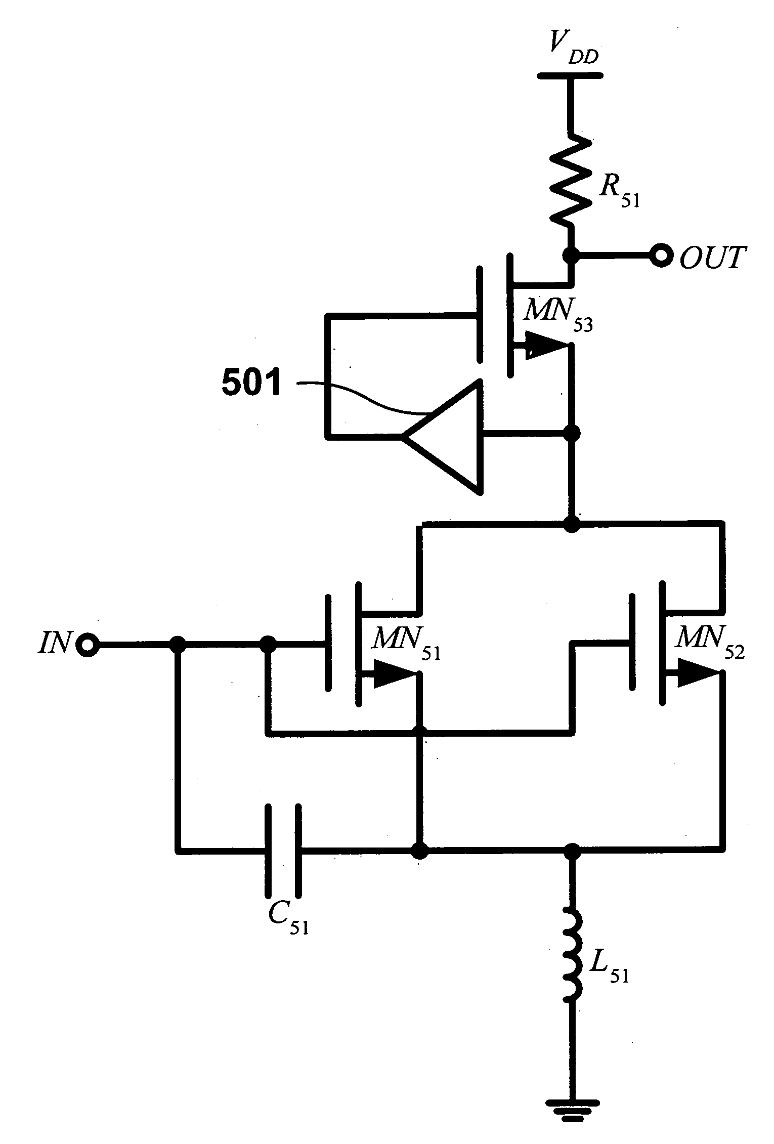
[0045]FIG. 5 is a circuit diagram of an amplifier circuit having improved linearity and frequency band using a MGTR according to the present invention. Referring to FIG. 5, the amplifier circuit includes transistors MN51, MN52 and M53, an inductor L51, a capacitor C51, a resistor R51, and a feedback amplifier 501. Since the basic configuration of the amplifier circuit of FIG. 4 is similar to that of the amplifier circuit of FIG. 3 and only the feedback amplifier part is different from the amplifier circuit of FIG. 3, only the feed-back amplifier 501 will now be explained.
[0046]The output port of the feedback amplifier 501 is connected to the gate of the transistor MN53 and the input port of the feedback amplifier 501 is connected to a node coupled to the source of the transistor MN53 and the drains of the MGTR MN51 and MN52. That is, the feedback amplifier 501 is added between the gate and source of the transistor MN53 to increase the impedance of a common gate input (input of the t...
PUM
 Abstract
Description
Claims
Application Information
 - R&D
- Intellectual Property
- Life Sciences
- Materials
- Tech Scout
- Unparalleled Data Quality
- Higher Quality Content
- 60% Fewer Hallucinations
Browse by: Latest US Patents, China's latest patents, Technical Efficacy Thesaurus, Application Domain, Technology Topic, Popular Technical Reports.
© 2025 PatSnap. All rights reserved.Legal|Privacy policy|Modern Slavery Act Transparency Statement|Sitemap|About US| Contact US: help@patsnap.com


