Method for interconnecting multi-layer printed circuit board

a printed circuit board and multi-layer technology, applied in the field of printed circuit boards, can solve the problems of complex process, difficult to form fine circuit patterns, difficult to obtain compact printed circuit boards,

Inactive Publication Date: 2008-01-22
LG INNOTEK CO LTD +1
View PDF11 Cites 11 Cited by
  • Summary
  • Abstract
  • Description
  • Claims
  • Application Information

AI Technical Summary

Benefits of technology

[0019]An object of the invention is to solve at least the above problems and/

Problems solved by technology

However, the above-described printed circuit board fabrication method has various disadvantages.
The process for coating the conductive paste should be repeatedly performed to form the conductor bump 2′ with the predetermined height, which results in a complicated process.
Accordingly, the adjacent conductor bumps are distanced from each other, which makes it difficult to form a fine circuit pattern or obtain a compact printed circuit board.
Moreover, in the repeated process of coating the conductive paste, an alignment process should be performed whenever the conductive paste is coated, which causes problems in that a productivity is degraded a

Method used


Image

  • Method for interconnecting multi-layer printed circuit board
  • Method for interconnecting multi-layer printed circuit board
  • Method for interconnecting multi-layer printed circuit board

Examples


Embodiment Construction

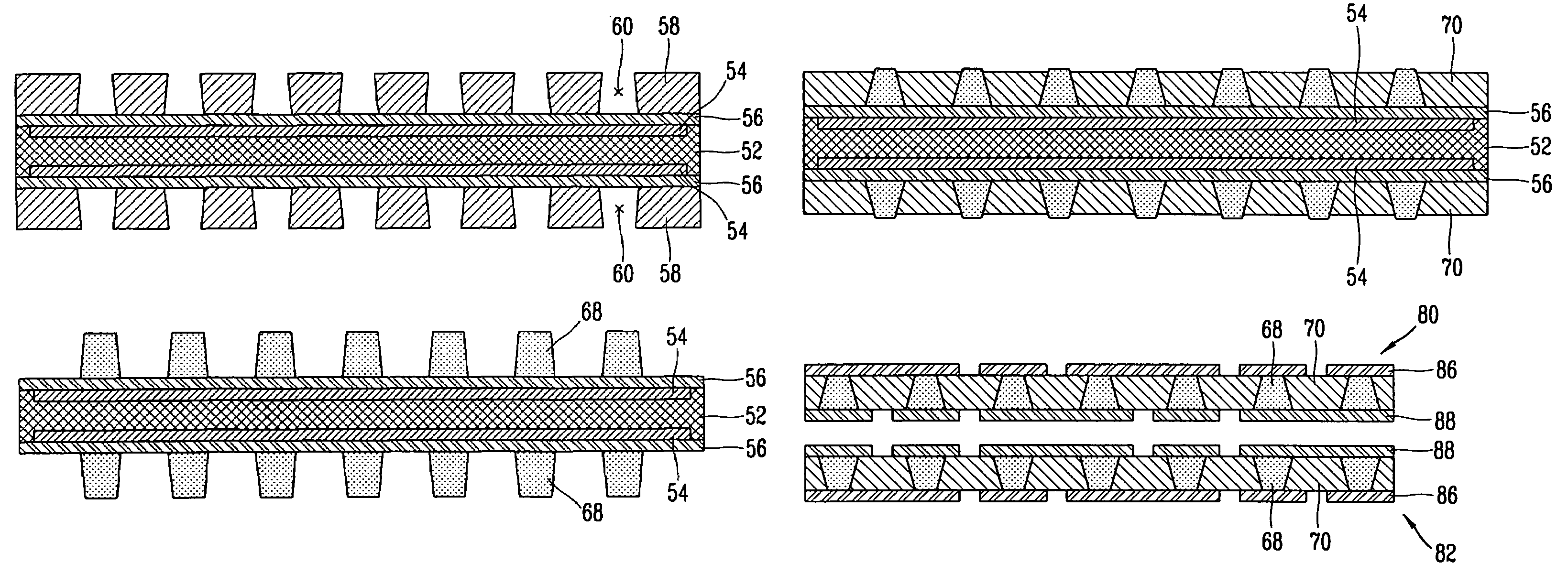
[0035]Reference will now be made in detail to the preferred embodiments of the present invention, examples of which are illustrated in the accompanying drawings. FIGS. 3A to 3J are diagrams showing a method for fabricating a printed circuit board in accordance with a first embodiment of the present invention.

[0036]As shown in FIG. 3A, a base material 50 is provided. The base material 50 can include releasing films 54 positioned at both sides of a base sheet 52 with a prescribed thickness and strength, and first metal thin films 56 stacked on both sides of the base sheet 52 with the releasing films 54 attached there between.

[0037]The releasing films 54 are preferably formed smaller than the base sheet 52 so that the edge of the first metal layers 56 are directly attached to the edge of the base sheet 52. However, the first metal layers 56 and the base sheet 52 are not in contact with each other at the portion where the releasing films 54 are stacked.

[0038]The base sheet 52 made of a ...


PUM

PropertyMeasurementUnit
Diameteraaaaaaaaaa
Strengthaaaaaaaaaa

Abstract

A method for fabricating a multi-layer printed circuit board can include forming an etching resist layer on a first metal layer having plating grooves that selectively expose the first metal layer, forming a plated layer at the surface of the first metal layer exposed by the plating groove through a plating process to form connection protrusion, removing the etching resist layer, forming an insulation layer at the first metal layer and positioning a second metal layer at the surface of the insulation layer coupled to an end portion of the connection protrusion. By forming the connection protrusion through the plating process, a loss of material can be reduced and a strength of the connection protrusion can be increased. Further, a complexity of the fabrication process is reduced to reduce costs and increase productivity.

Description

[0001]This application claims priority to Korean Application No. 7572 / 2003, filed Feb. 6, 2003 and claims the benefit of U.S. Provisional Application No. 60 / 463,322, filed Apr. 17, 2003. The entire disclosures of which are hereby incorporated by reference herein.BACKGROUND OF THE INVENTION[0002]1. Field of the Invention[0003]The present invention relates to a printed circuit board and, more particularly, to a method for interconnecting a multi-layer printed circuit board capable of electrically connecting circuit patterns stacked by multiple layers.[0004]2. Background of the Related Art[0005]FIG. 1 illustrates a conventional printed circuit board fabrication method that is disclosed in Korean Patent No. 203,540 (corresponding U.S. Pat. No. 5,600,103). As shown in FIG. 1, a process in which a conductive paste is coated on a copper foil pattern 3 by a screen printing method is repeatedly performed to obtain a conical conductor bump 2′ grown to a predetermined height. Then, a synthetic...

Claims


Application Information

Patent Timeline
IPC IPC(8): H05K3/02H05K3/10H05K3/00H05K3/42H05K3/46
CPCH05K3/423H05K3/0023Y10T29/49135H05K3/4647H05K2201/0355H05K2201/0394H05K2203/0346H05K2203/0577H05K2203/0733H05K2203/1536Y10T29/49126Y10T29/49147Y10T29/49156Y10T29/49155Y10T29/49128
Inventor LEE, SUNG-GUEHWANG, JUNG-HOHAN, JOON-WOOKLEE, SANG-MINEO, TAE-SIKYANG, YU-SEOCK
Owner LG INNOTEK CO LTD
Why Eureka
Try Eureka