Method of manufacturing liquid crystal display panels

a technology liquid crystal display panels, which is applied in the direction of instruments, electrical appliances, optics, etc., can solve the problems of reducing production efficiency, increasing manufacturing costs, and complicated operation of transporting the multiplicity of liquid crystal display panels to and from inspection apparatuses

Inactive Publication Date: 2008-01-22
SHARP KK
View PDF11 Cites 6 Cited by
  • Summary
  • Abstract
  • Description
  • Claims
  • Application Information

AI Technical Summary

Benefits of technology

[0018]According to the method of manufacturing liquid crystal display panels of the invention, at the process of forming a plurality of panels, the voltage can be applied to all of the LCD panel regions when the mother glasses are combined are have not been divided into individual liquid crystal display panels yet, which makes it possible to inspect display defects on the LCD panels, to perform a liquid crystal alignment stabilizing step utilizing a polymer or control the alignment with a simple apparatus.

Problems solved by technology

Therefore, when an operation of applying a voltage to individual liquid crystal display panels is performed after cutting the individual liquid crystal display panels from a mother glass as shown in FIGS. 13 and 14, an operation of transporting the multiplicity of liquid crystal display panels to and from an inspection apparatus becomes complicated.
Thus, the voltage applying process takes a long time to result in the problem of an increase in the manufacturing cost.
Further, since the voltage applying operation itself increases the number of manufacturing steps, it can reduce production efficiency.

Method used


Image

  • Method of manufacturing liquid crystal display panels
  • Method of manufacturing liquid crystal display panels
  • Method of manufacturing liquid crystal display panels

Examples


Embodiment Construction

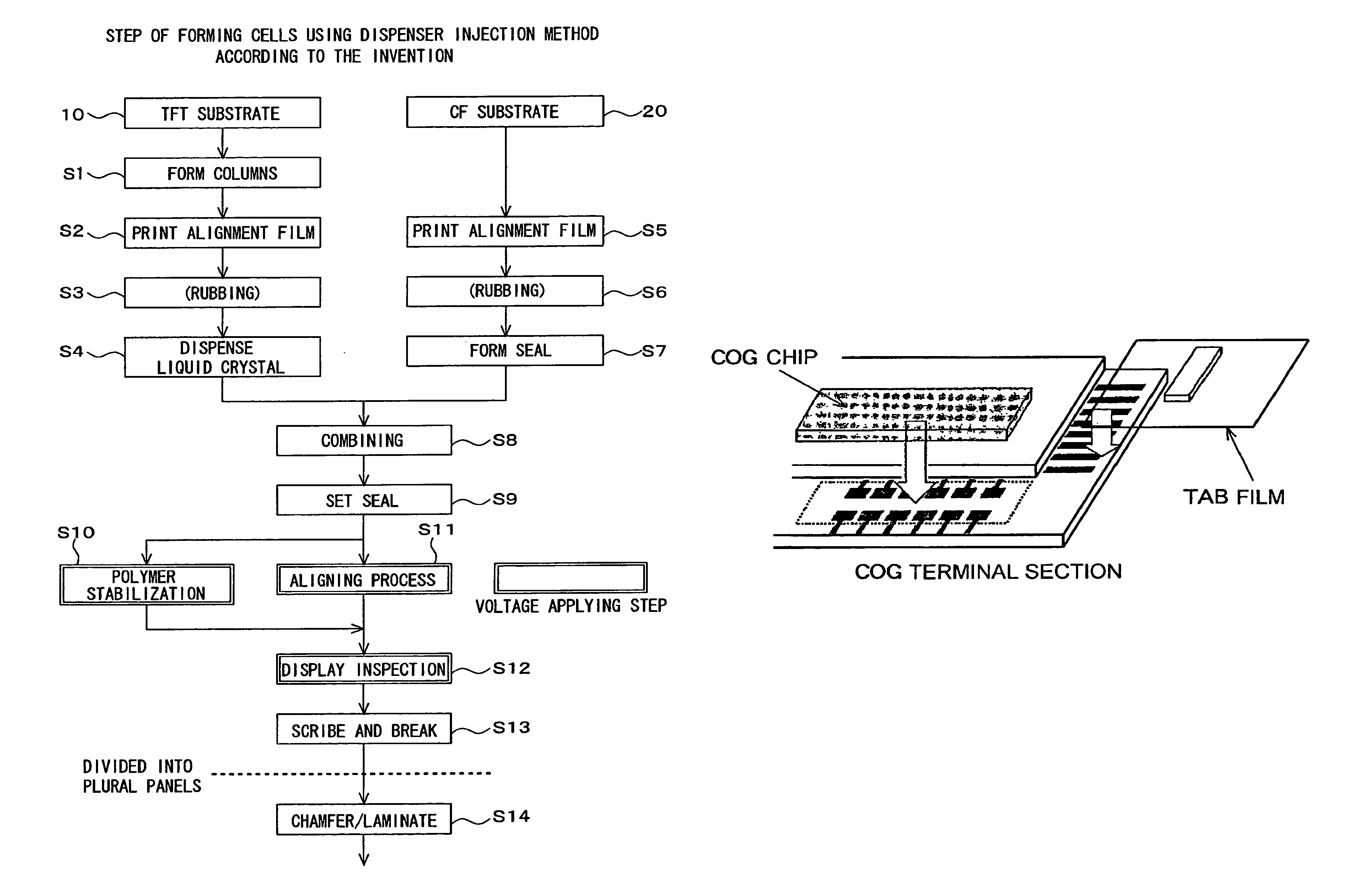
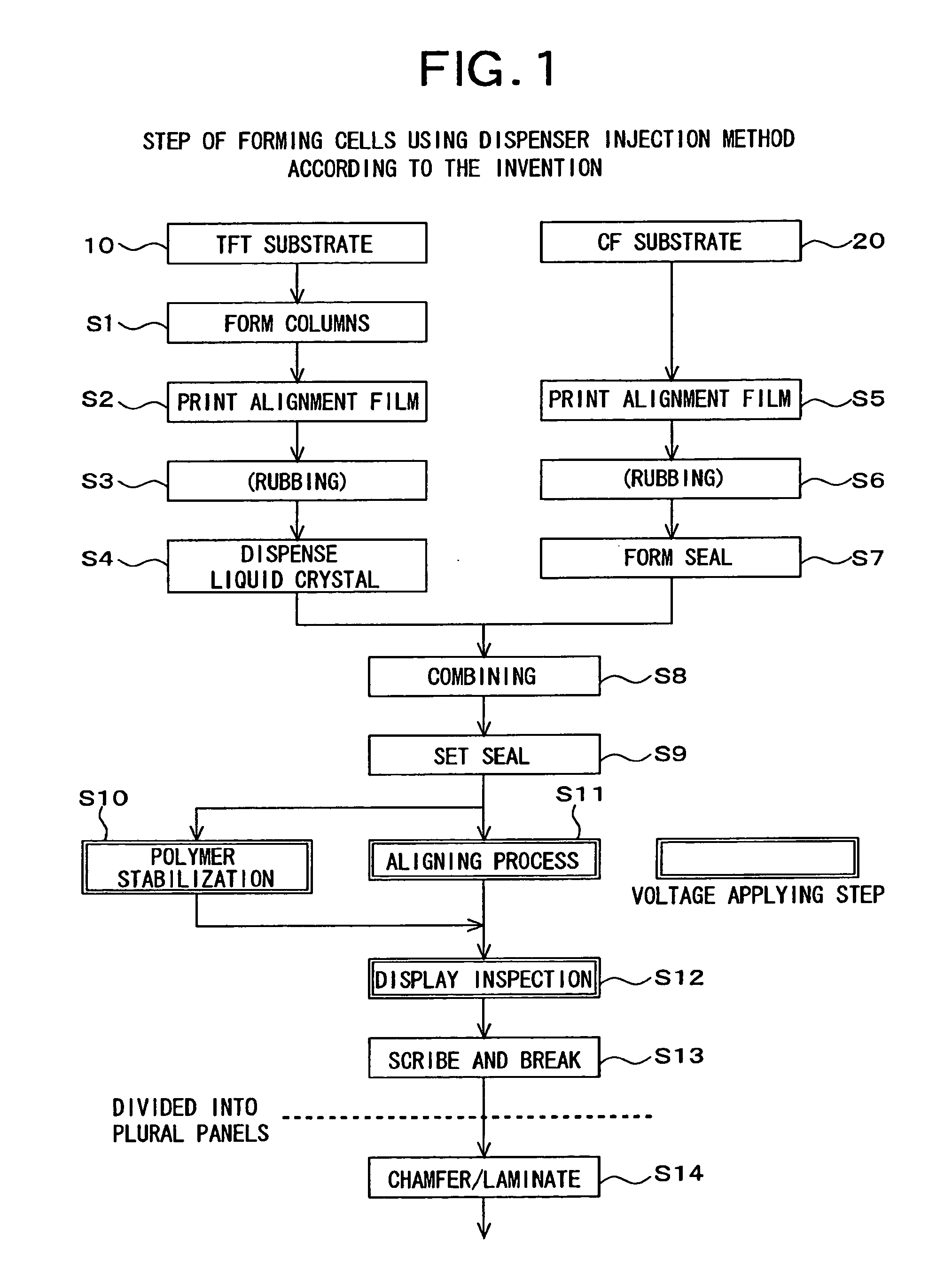
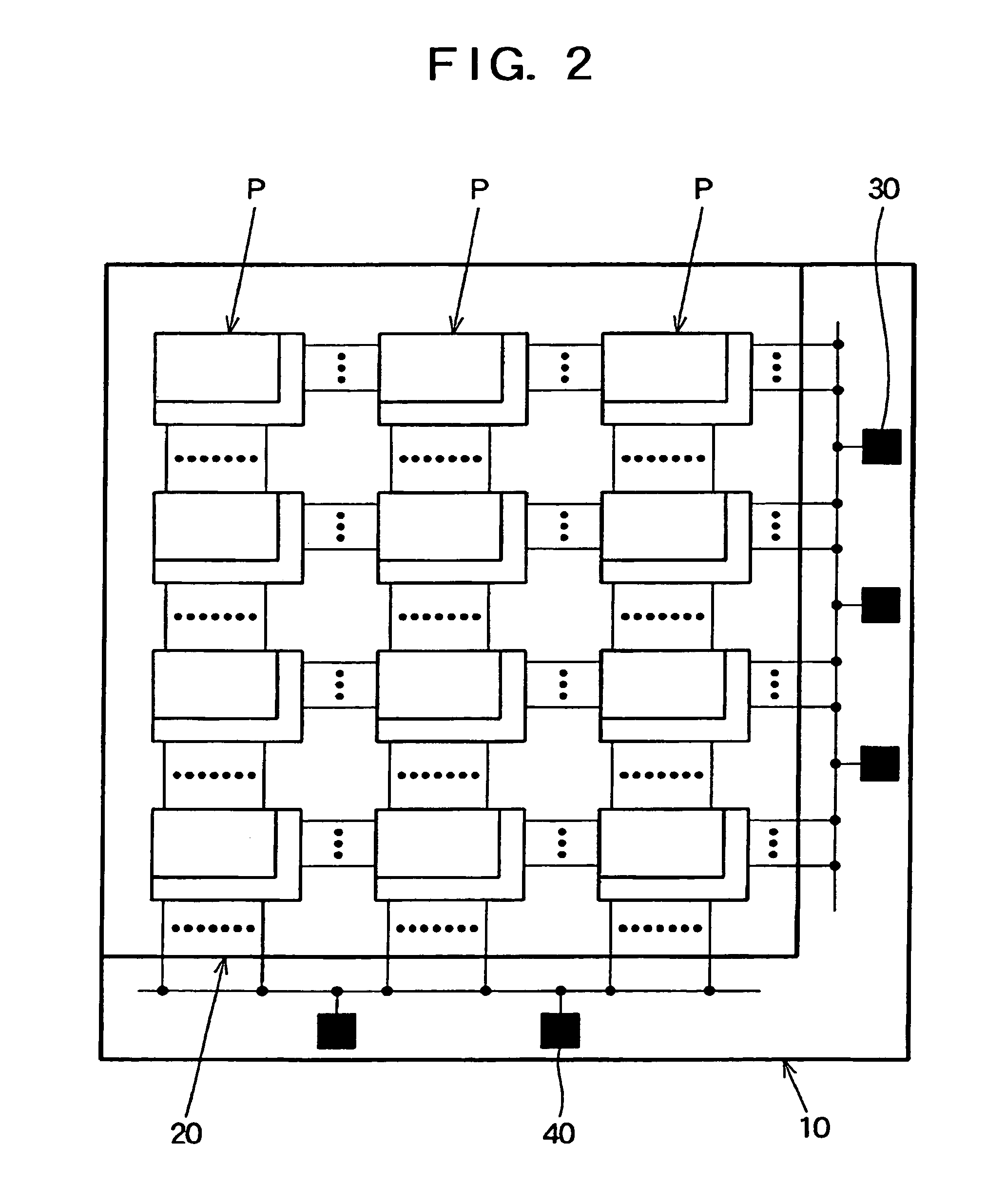
[0033]A method of manufacturing liquid crystal display panels according to an embodiment of the invention will now be described with reference to FIGS. 1 and 2. FIG. 1 is a flow chart showing steps of the method of manufacturing liquid crystal display panels in the present embodiment of the invention. For example, a glass substrate that is a transparent insulated substrate is used as a substrate 10 to serve as TFT substrates (a mother glass for TFT substrates) in FIG. 1. A multiplicity of TFT substrate regions are formed on the substrate 10 to serve as TFT substrates. A plurality of scan bus lines and a plurality of signal bus lines are provided in each of the TFT substrate regions such that they intersect each other with an insulation film interposed therebetween. A TFT (thin film transistor), a pixel electrode, and a storage capacitor electrode are formed in each of pixel regions which are defined by the bus lines. The TFTs function as switching elements for applying a gray scale ...


PUM

PropertyMeasurementUnit
voltageaaaaaaaaaa
sizesaaaaaaaaaa
angleaaaaaaaaaa

Abstract

Before cutting a gang-printed substrate having a multiplicity of liquid crystal display panel regions provided thereon into individual liquid crystal display panels, a voltage is applied to all of the multiplicity of liquid crystal display panel regions to inspect display defects, polymerize a monomer in the liquid crystal component, and control alignment of the liquid crystal, which allows the time required for a voltage applying step to be reduced and allows a reduction in the manufacturing cost. A dispenser injection process is used to allow a liquid crystal to be injected between mother boards that have not been cut into individual display panels, and a voltage is applied after the pair of glass substrates are combined and before they are cut into individual display panels to perform a test on display defects (dynamic operating test), pretilt control, and an aligning process.

Description

BACKGROUND OF THE INVENTION[0001]1. Field of the Invention[0002]The present invention relates to a method of manufacturing liquid crystal display panels (LCD panels) in which a multiplicity of liquid crystal display panels are cut and manufactured from a single glass substrate (mother glass) on a gang printing basis.[0003]2. Description of the Related Art[0004]FIG. 13 shows a flow of steps for manufacturing liquid crystal display panels according to the related art utilizing a vacuum injection process. Among the steps for manufacturing liquid crystal display panel, the vacuum injection process is used for sealing a liquid crystal between two glass substrates facing each other by combining the two glass substrates having pixel electrodes, or a common electrode and various lines formed thereon with a predetermined gap left therebetween and injecting the liquid crystal in the gap through an opening provided at a combined end section in a vacuum atmosphere.[0005]In the case of multi-sho...

Claims


Application Information

Patent Timeline
Patent Type & Authority Patents(United States)
IPC IPC(8): H01L21/00G02F1/13G02F1/1333G02F1/1337G02F1/137G02F1/139G02F1/141
CPCG02F1/133351G02F2001/13775G02F1/141G02F1/1393G02F1/13775
Inventor TANAKA, YOSHINORIMARUYAMA, YOSHIAKI
Owner SHARP KK
Why Eureka
Try Eureka