Stack structure with semiconductor chip embedded in carrier

a technology of semiconductor chips and stack structures, which is applied in the direction of stacked and attached pcbs, printed circuit aspects, electrical apparatus construction details, etc., can solve the problems of inability to achieve the purpose of being slim and small, increased fabrication costs, and complicated processes as such, so as to reduce the size of the module, and increase the flexibility of changing combinations

Active Publication Date: 2008-01-22
PHOENIX PRECISION TECH CORP
View PDF9 Cites 133 Cited by
  • Summary
  • Abstract
  • Description
  • Claims
  • Application Information

AI Technical Summary

Benefits of technology

[0008]Another objective of the present invention is to provide a stack structure with semiconductor chips embedded in a carrier to flexibly change the number of semiconductor chips based upon demands, so as to provide a greater flexibility on changing combinations.
[0009]Still another objective of the present invention is to provide a stack structure with semiconductor chips embedded in a carrier, so as to reduce the size of the module.
[0010]In accordance with the above-mentioned and other objectives, the present invention proposes a stack structure with semiconductor chips embedded in a carrier, mainly comprising: two carriers having at least one cavity formed thereon respectively and being stacked as a whole by a linking layer; at least two semiconductor chips placed in the cavity of the carriers respectively, wherein the semiconductor chips respectively comprise an active surface with a plurality of electrically connecting pads formed thereon and an inactive surface corresponding to the active surface; at least one dielectric layer formed on the active surface of the semiconductor chip and the surface of the carrier, wherein at least an opening is formed in the dielectric layer at a position corresponding to the top of the electrode pad; at least one circuit layer formed on the surface of the dielectric layer and at least a conductive structure formed in the opening of the dielectric layer, wherein the circuit layer is electrically connected to the electrode pad of the semiconductor chip by the conductive structure. The carriers are stacked with a linking layer formed therebetween so as to form a module structure allowing the combinations and the amounts of semiconductor chips to be changed flexibly, in order to meet the demands of different alternation with a greater flexibility on changing combinations.
[0011]The semiconductor chips are placed in the cavities of the carriers and then the carriers are stacked together having the active surface of the semiconductor chip and the surface of the carrier formed with a dielectric layer, a circuit layer and a conductive structure electrically connected to the electrode pad of the semiconductor chip, so as to form a stack module structure to avoid the thickness increment resulted from directly stacked up caused in prior art and the defects of wire bounding to reduce the size to achieve the purpose for being slim and small.

Problems solved by technology

Since the height of the package is increased by the height of the arc line of the wire bond type structure, the purpose of being slim and small is thus unable to achieve.
Moreover, the semiconductor chips 121 and 122 are electrically connected by the bonding layer 13 in chip-level, that is to say, the stacking process of the semiconductor chips 121 and 122 must be done in a semiconductor factory (wafer foundry) before having the packaging process being done in a semiconductor package factory, thus the process as such is more complicated and the cost of fabrication is increased.
However, to reduce the area of circuit board by the fine circuit has a limited effect; and to improve the electric performance and the performance of modularization by directly stacking the semiconductor chips 121 and 122 is unfavorable as it may not be able to expand continuously due to the limited amount of the stacked chips, thus the purpose of being slim and small is also unfeasible.
In this regard, to increase the chip density placed on a multi-layer circuit board and decrease the area occupied by the semiconductor chips on the multi-layer circuit board for reducing the size of the package to improve the storage capacity have become an important issue in the circuit board industry.

Method used


Image

  • Stack structure with semiconductor chip embedded in carrier
  • Stack structure with semiconductor chip embedded in carrier
  • Stack structure with semiconductor chip embedded in carrier

Examples


first preferred embodiment

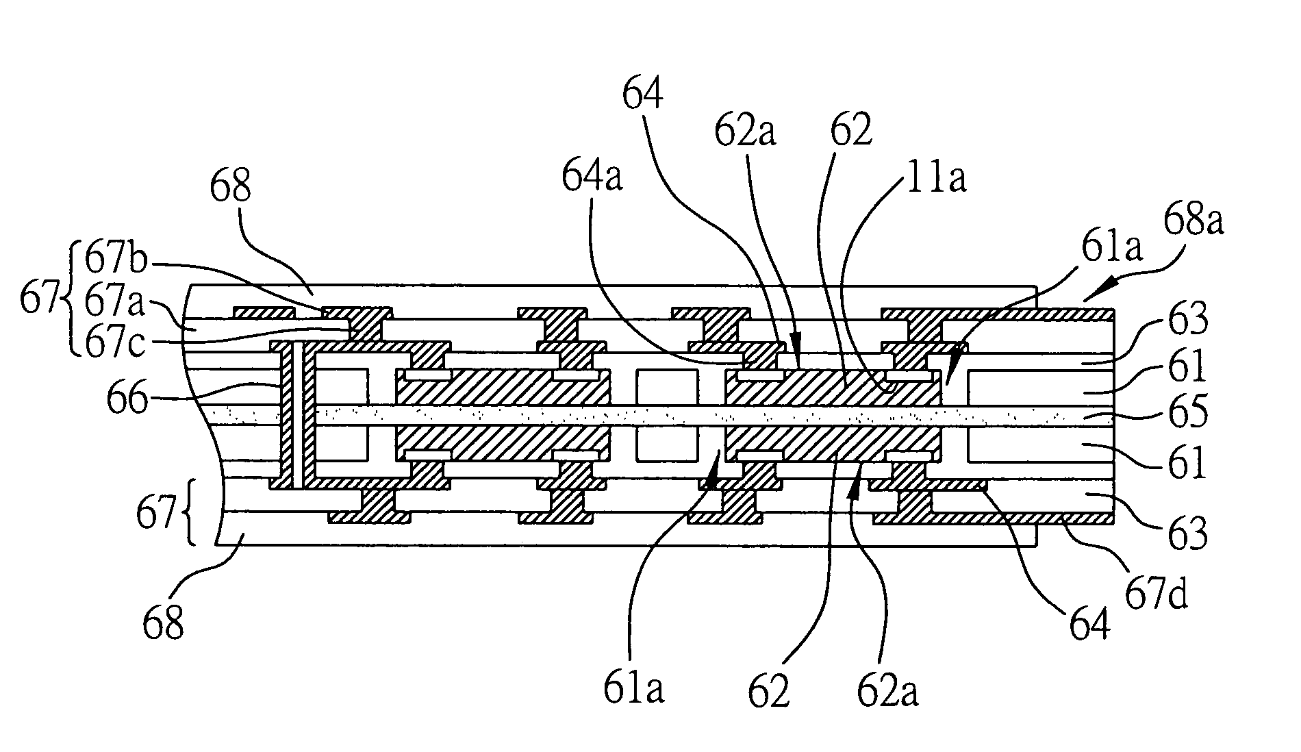
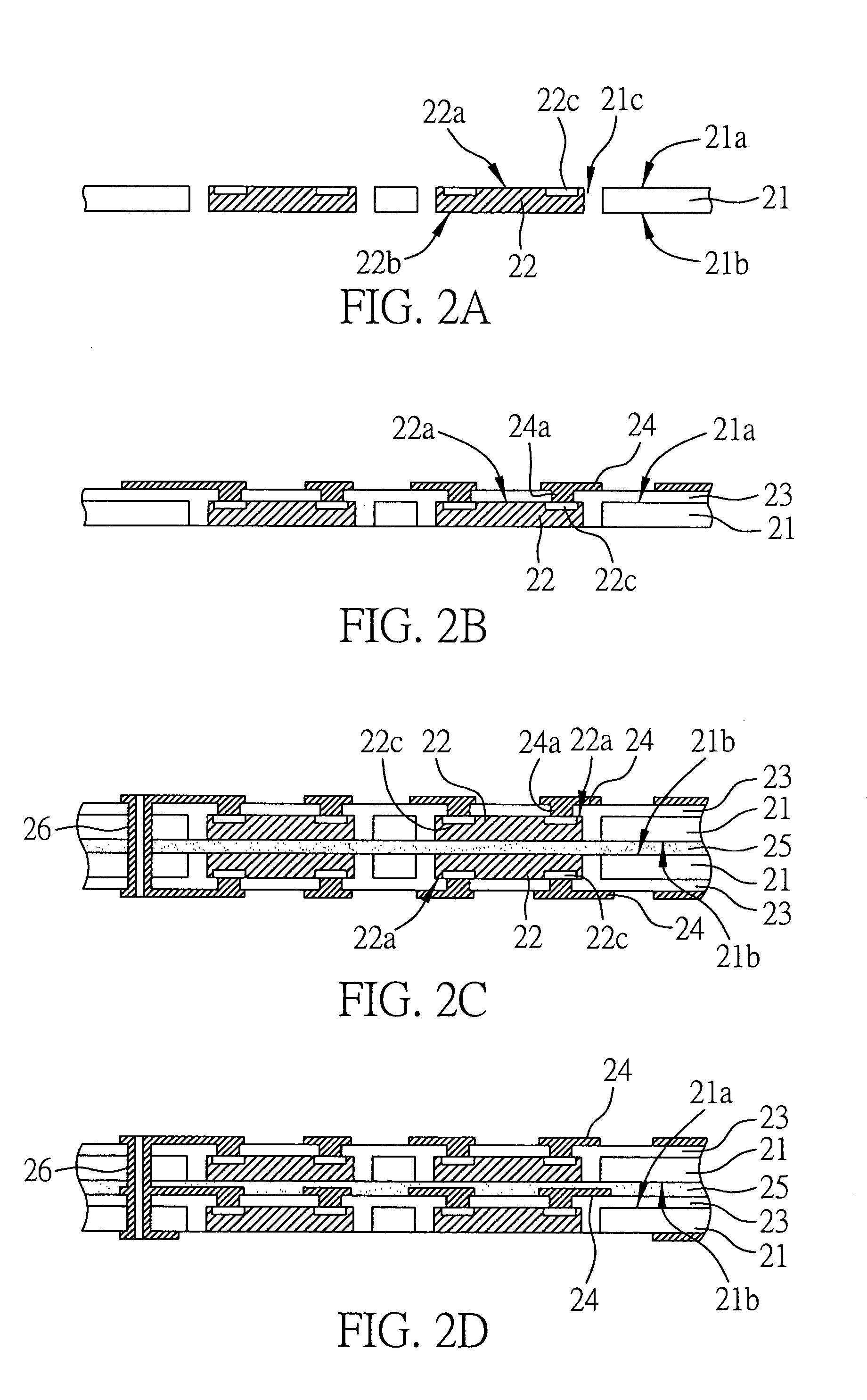
[0023]Referring to FIG. 2A to 2C, crossing-sectional views showing a stack structure with semiconductor chips embedded in a carrier according to the present invention are provided.

[0024]FIG. 2A shows at least two carriers 21, respectively, having a first surface 21a and a second surface 21b with at least a cavity 21c formed on the carrier 21 that is penetrated through the first and the second surfaces 21a and 21b, wherein the carrier 21 is an insulating board or a circuit board with circuits. The cavity 21c has at least a semiconductor chip 22 placed therein by an adhesive material (not shown) fastening the semiconductor chip 22 in the cavity 21c of the carrier 21. The semiconductor chip 22 is at least one of the group of active components and the group of passive components, wherein the active components may be a memory and the passive components may be an electronic component such as a resistor, a capacitor, an inductor. or the like. Further, the semiconductor chip 22 comprises an...

second preferred embodiment

[0029]Referring to FIGS. 3A and 3B, cross-sectional views showing a stack structure with semiconductor chips embedded in a carrier according to another embodiment of the present invention are provided, wherein it is distinguished from the foregoing embodiment by having the active surfaces of the semiconductor chips embedded in the cavity of the carrier in different directions.

[0030]Referring to FIG. 3A, a plurality of cavities 31c of the carrier 31 have respectively semiconductor chips 32 placed therein. It may be achieved by employing an adhesive material (not shown) to secure the semiconductor chip 32 to the cavity 31c of the carrier 31, wherein the active surface 32a of the semiconductor chip 32 is selectively formed on the first surface 31a and the second surface 31b of the carrier 31, so that the first and the second surfaces 31a and 31b of the carrier 31 have the active surfaces 32a of the semiconductor chips 32 respectively.

[0031]Referring to FIG. 3B, the first and the second...

third preferred embodiment

[0033]Referring to FIGS. 4A and 4B, cross-sectional views showing a stack structure with semiconductor chips embedded in a carrier according to another embodiment of the present invention are provided, wherein it is distinguished from the foregoing embodiment by having a cavity 41c of a carrier 41 that is non-through. The direction of the cavities 41c are selectively formed on the first surface 41a or the second surface 41b of the carrier 41. The semiconductor chips 42 may be placed in the cavity 41c with the active surfaces 42 of the semiconductor chips 42 facing the same direction or different direction. The dielectric layer 43 and the circuit layer 44 having the conductive structures 44a are formed on the active surface 42a of the semiconductor chip 42 and the surface of the carrier 41, wherein the conductive structures 44a are electrically connected to the electrode pads 42b of the semiconductor chip 42, thereby reducing the overall size of the stack structure achieving the fore...


PUM


Abstract

A stack structure with semiconductor chips embedded in carriers comprises two carriers stacking together as a whole, at least two semiconductor chips having active surfaces with electrode pads and inactive surfaces corresponding thereto placed in the cavities of the carriers, at least one dielectric layer formed on the active surface of the semiconductor chip and the surface of the carrier, at least a conductive structure formed in the opening of the dielectric layer, and at least a circuit layer formed on the surface of the dielectric layer wherein the circuit layer is electrically connected to the electrode pad by the conductive structure, so as to form a three-dimensional module to increase the storage capacity dramatically and integrate the semiconductor chips in the carriers for efficiently reducing the size of the module, so that the combinations can be changed flexibly to form the required storage capacity according to the demands.

Description

FIELD OF THE INVENTION[0001]The present invention relates to stack structures of semiconductor chips embedded in carriers, and more particularly, to a stack structure having one or more semiconductor chips embedded in one or more carriers before stacking the carriers together.BACKGROUND OF THE INVENTION[0002]Due to the rapid development of electronic technology, electronic products with multi-functions and high performances have been developed so as to satisfy the demand of high integration and miniaturization of semiconductor packaging and to improve the storage capacity and performance of the semiconductor package, in order to accommodate tendency of the miniaturization, large storage capacity and high speed of electronic products. In prior art, most of the semiconductor packages are fabricated by the Multi Chip Module (MCM) technology. Such packing technology allowing the size of the package to be reduced and the electric performance to be improved has thereby become a mainstream...

Claims


Application Information

Patent Timeline
Patent Type & Authority Patents(United States)
IPC IPC(8): H01L23/02H01L23/34
CPCH01L23/5389H01L24/82H01L25/105H05K1/185H01L24/24H01L2224/73267H01L2224/24227H01L2224/48091H01L2924/01078H01L2924/01079H01L2924/15153H01L2924/15165H01L2924/1517H01L2924/19041H01L2924/19042H01L2924/19043H01L2924/30105H05K3/4602H05K3/4611H05K2201/043H05K2201/10515H05K2201/10674H01L2225/1058H01L2224/45144H01L2224/73265H01L2924/014H01L2924/01033H01L2924/01006H01L2924/01005H01L24/48H01L2924/00014H01L2924/00H01L2224/04105H01L24/45H01L2924/181H01L2924/00015H01L2224/05599H01L2924/00012
Inventor HSU, SHIH-PING
Owner PHOENIX PRECISION TECH CORP
Why Eureka
Try Eureka