Acceleration sensor with redundant contact holes

a contact hole and acceleration sensor technology, applied in the direction of speed/acceleration/shock measurement, semiconductor devices, instruments, etc., can solve the problems of shortening the life of the sensor, affecting the accuracy of the sensor, so as to achieve sensitive and reliable results

Active Publication Date: 2008-01-29
LAPIS SEMICON CO LTD
View PDF6 Cites 56 Cited by
  • Summary
  • Abstract
  • Description
  • Claims
  • Application Information

AI Technical Summary

Benefits of technology

[0011]A general object of the present invention is to provide an acceleration sensor that is both sensitive and reliable.
[0012]A more specific object is to enhance the sensor's immunity to electrical faults in contact holes formed in high-stress areas.
[0014]The invented acceleration sensor has an extended life expectancy because it can survive an electrical fault in one contact hole without significant alteration of its electrical characteristics, provided adequate electrical contact is maintained in at least one other contact hole. The provision of multiple contact holes also facilitates the meeting of contact resistance tolerances.
[0015]The contact holes are preferably aligned in the longitudinal direction of the beam, so that stress from the bending of the beam will cause a failure in only one contact hole at a time. This arrangement also enables the width of the beams to be reduced.

Problems solved by technology

At these locations, however, a large mechanical stress also acts on the interface between the wiring in the contact holes and the silicon surfaces of the piezoelectric resistive elements 15-1, 15-2, and can produce such unwanted effects as wire peeling and separation, which degrade the reliability and shorten the life of the sensor.
Variations in contact resistance can therefore quickly push the resistance value above the tolerance level, so that the sensor does not perform as designed.
These problems have a serious effect on sensor life and reliability.
In addition, the anticipated reduction of contact hole sizes and the attendant increased variation in contact resistance values will have a serious effect on future sensor performance.

Method used


Image

  • Acceleration sensor with redundant contact holes
  • Acceleration sensor with redundant contact holes
  • Acceleration sensor with redundant contact holes

Examples


Embodiment Construction

[0031]An embodiment of the invention will now be described with reference to the attached drawings, in which like elements are indicated by like reference characters.

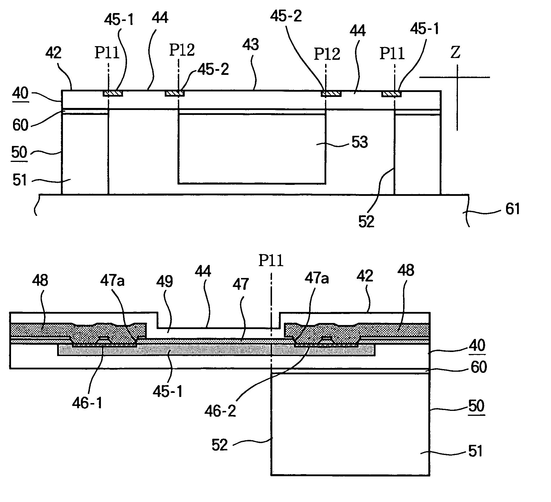
[0032]Referring to FIG. 4, a piezoelectric three-axis acceleration sensor is formed by etching a silicon-on-insulator wafer comprising a first silicon layer 40 approximately five to ten micrometers (5 to 10 μm) thick and a second silicon layer 50 approximately 525 μm thick joined by a bonding layer 60 such as a buried silicon oxide layer (BOX layer) approximately 5 μm thick. The first silicon layer 40 is a semiconductor silicon layer doped with an n-type impurity and has a volume resistivity of about six to eight ohm-centimeters (6 to 8 Ω·cm). The second silicon layer 50 is a silicon substrate layer having a volume resistivity of about 16 Ω·cm.

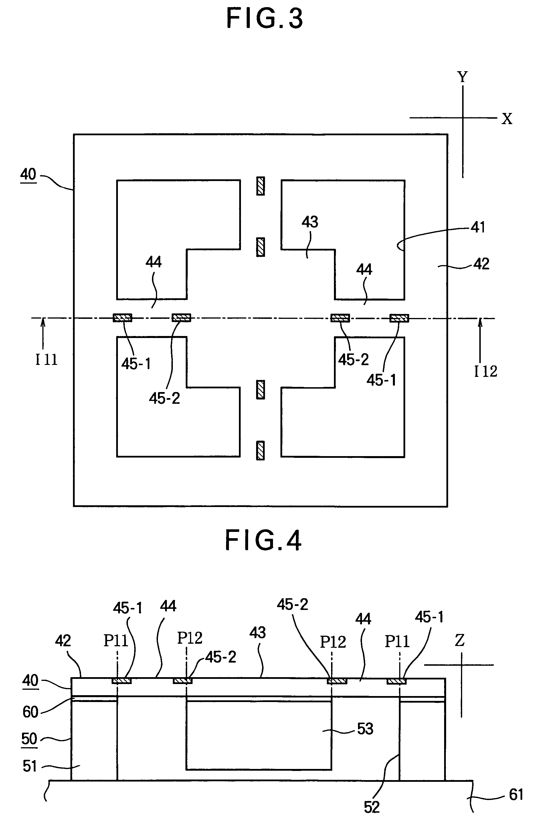
[0033]Referring to FIG. 3, the first silicon layer 40 for one acceleration sensor is substantially square with sides approximately two and a half millimeters (2.5 mm) long, compri...


PUM


Abstract

An acceleration sensor includes a mass and a supporting member linked by a flexible beam. A strain detector having low-resistance areas at both ends is formed near a boundary between the beam and the mass or between the beam and the supporting member. A dielectric film formed on the supporting member and the beam has multiple contact holes disposed over each low-resistance area. Wiring formed on the dielectric film is connected to the low-resistance areas through the contact holes. The provision of multiple contact holes for each low-resistance area extends the life of the acceleration sensor by preventing sensor failure due to the separation or other failure of any single contact.

Description

BACKGROUND OF THE INVENTION[0001]1. Field of the Invention[0002]The present invention relates to a three-axis acceleration sensor, more particularly to technology for preventing faulty electrical contacts at the acceleration detection sites.[0003]2. Description of the Related Art[0004]Technology for detecting acceleration on three mutually orthogonal axes is described in, for example, Japanese Patent Application Publication No. 2004-198243. A piezoelectric acceleration sensor of the type disclosed in this Publication is shown schematically in FIGS. 1 and 2. FIG. 1 shows a plan view; FIG. 2 shows a sectional view through line I1-I2 in FIG. 1.[0005]This acceleration sensor has a thin square first silicon layer 10, a thick square second silicon layer 20, and a bonding layer 30 by which the first and second silicon layers are joined. Substantially L-shaped openings 11 at the inside four corners of the first silicon layer 10 create a frame-shaped peripheral attachment section 12, a squar...

Claims


Application Information

Patent Timeline
Patent Type & Authority Patents(United States)
IPC IPC(8): G01P15/12G01P15/18H01L29/84
CPCG01P15/18G01P15/123G01P2015/084G01P15/09
Inventor KAI, TAKAYUKI
Owner LAPIS SEMICON CO LTD
Why Eureka
Try Eureka