Process for depositing a layer of material on a substrate

a technology of substrate and material, applied in the direction of electrolysis components, cell components, coatings, etc., can solve the problems of robbery of the plate and destructive removal

Inactive Publication Date: 2008-01-29
VLSI TECH LLC
View PDF27 Cites 22 Cited by
  • Summary
  • Abstract
  • Description
  • Claims
  • Application Information

AI Technical Summary

Problems solved by technology

This nonuniform deposition causes problems, particularly if the plated material 26 is to be chemically mechanically polished.
The robber plate is attached to the board and is destructively removed by cutting the piece of the board having the robber plate.

Method used


Image

  • Process for depositing a layer of material on a substrate
  • Process for depositing a layer of material on a substrate
  • Process for depositing a layer of material on a substrate

Examples


Embodiment Construction

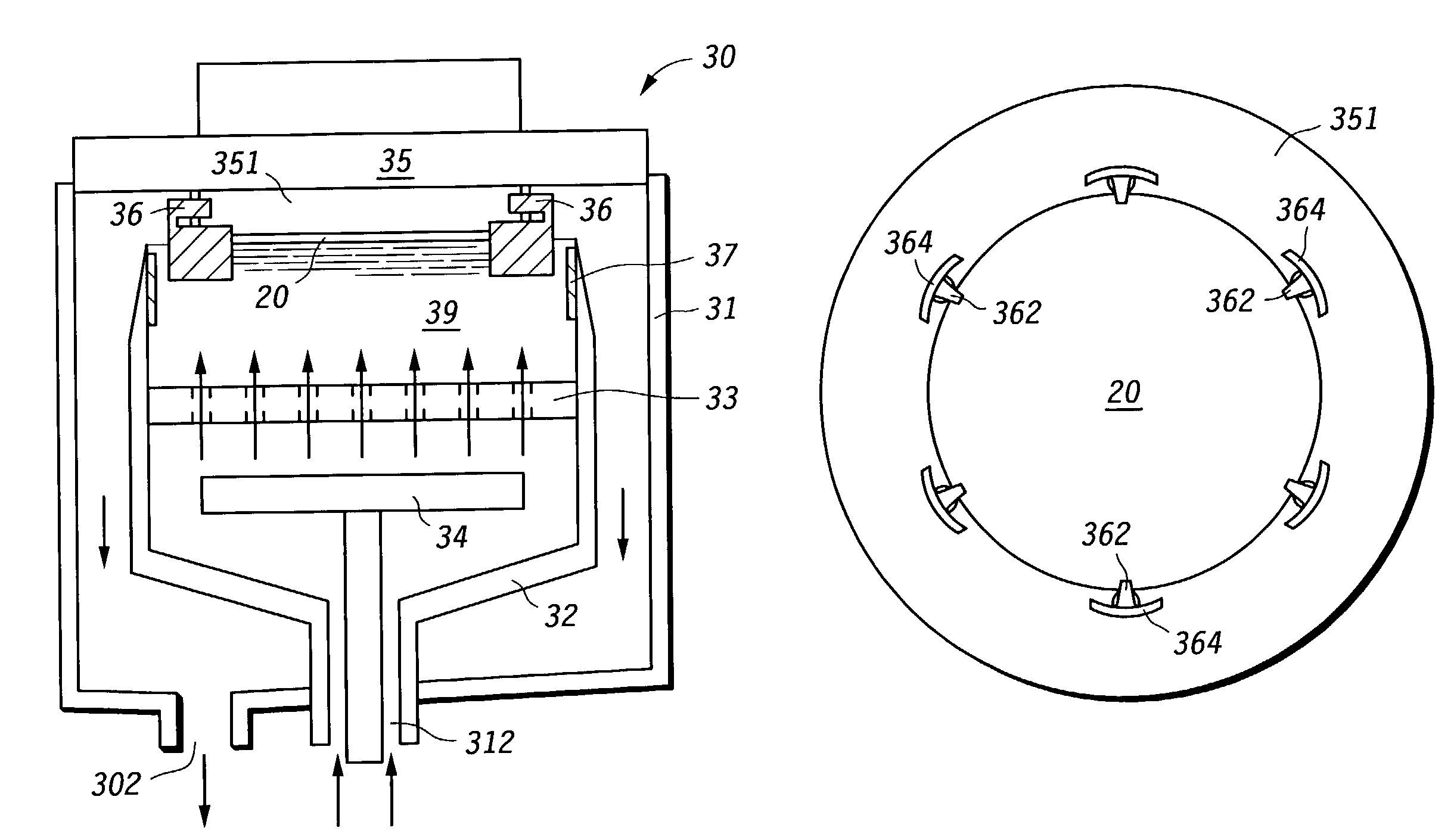
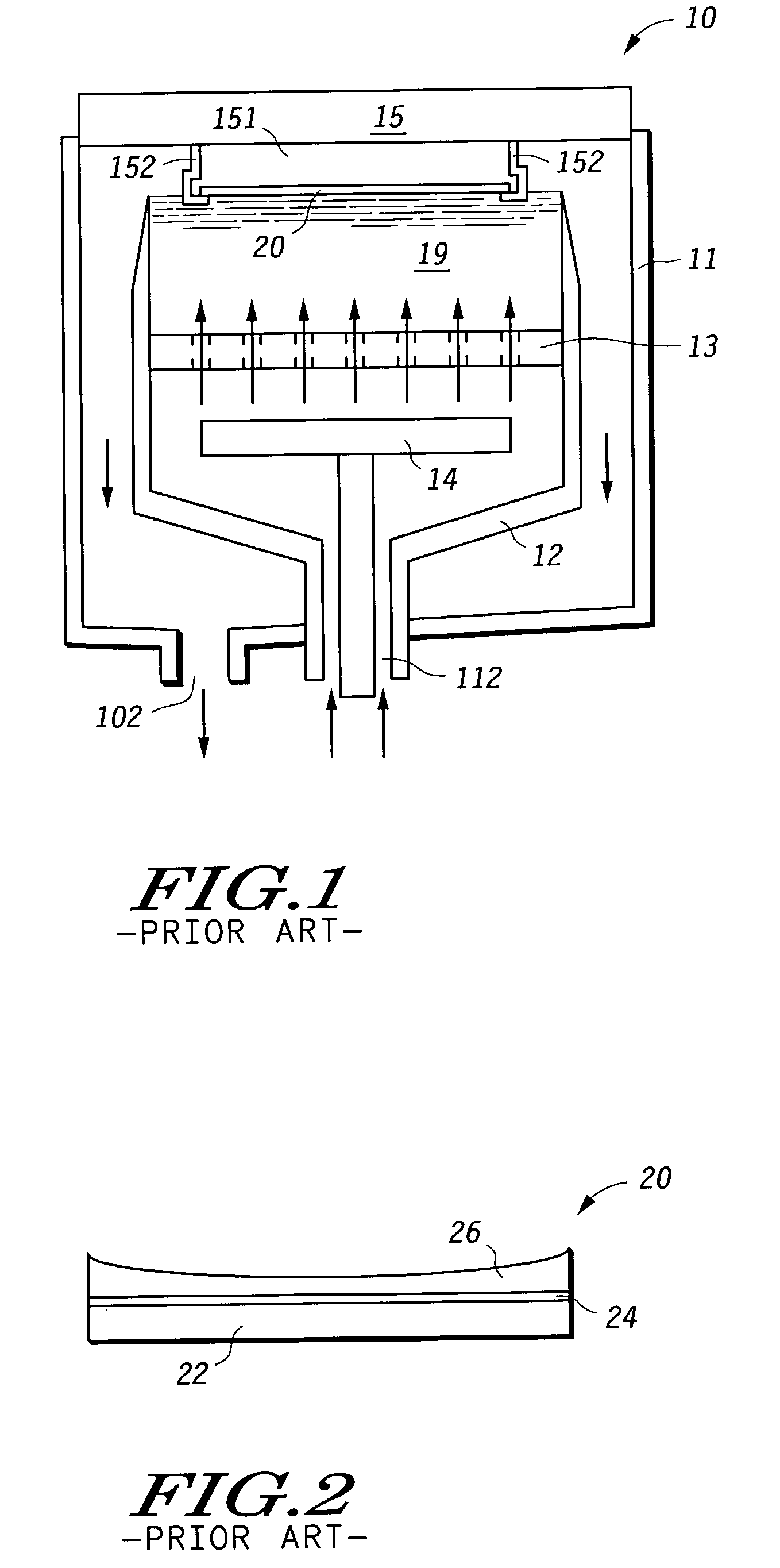
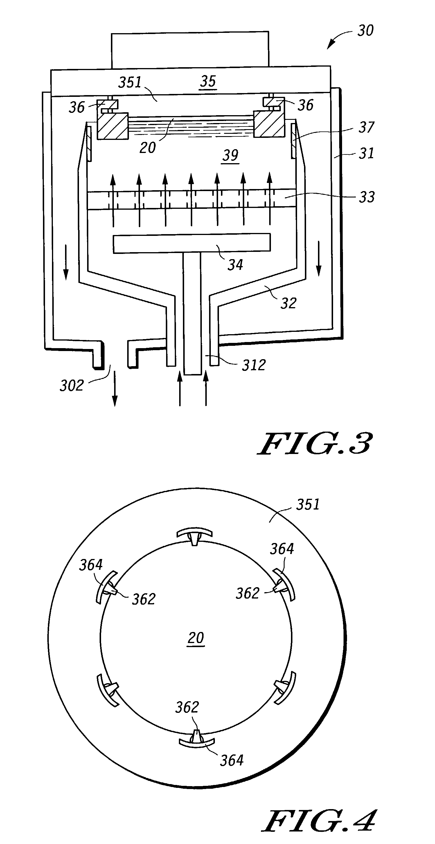
[0016]A new electroplating system and process makes the electrical current density across a semiconductor device substrate surface more uniform during plating to allow for a more uniform or tailored deposition of a conductive material. The electrical current density modifiers reduce the electrical current density near the edge of the substrate where the plating rate would otherwise be the highest. By reducing the current density near the edge of the substrate, the plating becomes more uniform or can be tailored so that slightly more material is plated near the center of the substrate. The system can also be modified so that the material that current density modifier portions on clamping structures can be removed without having to disassemble any portion of the head or otherwise remove the arc-shaped electrical current density modifier from the system. This in-situ cleaning reduces the amount of equipment downtime, increases equipment lifetime, and reduces particle counts.

[0017]FIG. ...


PUM

PropertyMeasurementUnit
arc lengthaaaaaaaaaa
heightaaaaaaaaaa

Abstract

An electroplating system (30) and process makes electrical current density across a semiconductor device substrate (20) surface more uniform during plating to allow for a more uniform or tailored deposition of a conductive material. The electrical current density modifiers (364 and 37) reduce the electrical current density near the edge of the substrate (20). By reducing the current density near the edge of the substrate (20), the plating becomes more uniform or can be tailored so that slightly more material is plated near the center of the substrate (20). The system can also be modified so that the material that plates on electrical current density modifier portions (364) of structures (36) can be removed without having to disassemble any portion of the head (35) or otherwise remove the structures (36) from the system. This in-situ cleaning reduces the amount of equipment downtime, increases equipment lifetime, and reduces particle counts.

Description

[0001]This Application is based on and is a division of prior U.S. patent application Ser. No. 09 / 561,776, filed on May 1, 2000, now U.S. Pat. No. 6,500,324, which is a division of U.S. patent application Ser. No. 08 / 856,459, filed on May 14, 1997, now U.S. Pat. No. 6,174,425, which are hereby incorporated by reference, and priority thereto for common subject matter is hereby claimed.FIELD OF THE INVENTION[0002]This invention relates in general to processes and systems for depositing layers on substrates, and more particularly, processes and systems for electroplating metal-containing layers on those substrates.BACKGROUND OF THE INVENTION[0003]Currently semiconductor devices are requiring higher current densities for operation while still resisting electromigration or other reliability problems. Copper is being investigated as being a possible alternative to current aluminum or aluminum-copper metalization. One of the most promising methods of depositing copper on a substrate is by ...

Claims


Application Information

Patent Timeline
Patent Type & Authority Patents(United States)
IPC IPC(8): C25D5/48C25D21/00C25D7/12C25D5/00C25D7/00C25D17/00H01L21/288
CPCC25D5/00H01L21/2885C25D17/008C25D7/123C25D3/665C25D17/001C25D5/04C25D5/18C25D21/00Y10S204/07
Inventor SIMPSON, CINDY REIDSEMAHERRICK, MATTHEW T.ETHERINGTON, GREGORY S.LEGG, JAMES DEREK
Owner VLSI TECH LLC
Why Eureka
Try Eureka