Method of layer transfer comprising sequential implantations of atomic species

a layer transfer and atomic species technology, applied in the field of crystalline wafers, can solve the problems of requiring implantation time, blisters tend to form at the bonded interface, and require a long time to implantation, and achieve the effects of low surface roughness, limited blister formation, and optimal thickness uniformity

Inactive Publication Date: 2008-01-29
SOITEC SA
View PDF14 Cites 18 Cited by
  • Summary
  • Abstract
  • Description
  • Claims
  • Application Information

AI Technical Summary

Benefits of technology

[0017]A preferred embodiment of the present invention relates to a method of manufacturing a crystalline wafer that includes implanting first atomic species in a donor substrate to form a region of weakness at a first depth therein and configured to facilitate detachment of a first layer of the donor substrate from a remaining portion of the donor substrate. The first layer and remaining portion are disposed on opposite sides of the region of weakness. The preferred embodiment also includes implanting second atomic species in the donor substrate to form a gettering region at a second depth therein that is different than the first depth, and bonding a handle substrate to the donor substrate to provide a bonded structure having a bonded interface. The gettering region is configured to reduce or minimize migration of the implanted first atomic species past the gettering region to reduce or minimize the formation of blisters at the bonded interface. Preferably, the method further includes applying energy at the region of weakness to detach the first layer from the remaining portion, and to transfer the first layer to the handle substrate.
[0019]Preferably, the gettering region is configured to reduce or minimize the formation of blisters at the bonded interface by capturing implanted first atomic species that migrate from the region of weakness. The gettering region is preferably insufficiently weak to cause detachment of the donor substrate at the gettering region upon application of energy at the region of weakness. Additionally, the second depth is selected such that the gettering region is positioned in the donor substrate between the region of weakness and the bonded interface.
[0026]The invention thus provides a method for producing a structure that includes a thin layer of semiconductor material on a substrate which exhibits at the same time limited blister formation, low surface roughness, and an optimal thickness uniformity.

Problems solved by technology

This reduction of required dose translates to a reduction in the required implantation time, and also to costs associated with production of wafer structures comprising a thin layer on a handle substrate, in particular by means of a transfer process, such as Soitec's SMART-CUT® process.
Co-implantation of atomic species, however, also presents a disadvantage that blisters tend to form at the bonded interface between the free surface of the implanted donor substrate under which implantation has been carried out and the surface of the handle substrate.
It is known that blisters tend to form after a co-implantation of atomic species, for example helium and hydrogen species, because helium species may diffuse in the matrix of the donor substrate more easily than hydrogen species, and the risk of blister formation increases if helium is implanted close to the bonded interface.
The appearance of blisters at the bonded interface may effectively lead to the degradation of the bonded interface.
Hence, when a SMART-CUT® process is carried out, blisters that form at the bonded interface may disturb the structural properties of the thin layer which has been detached.
Blisters may even cause a detachment at the level of the blister sites, that is at the level of the bonded interface and not at the level of the region of weakness, thus creating “non-transferred” zones and introducing roughness and structural defects to the transferred thin layer.
Structures presenting non-transferred zones are usually rejected from the production line, and hence decrease the production yield.
Additionally, blisters and voids have also been observed to some extent when an implantation is carried out by implanting a single atomic species within a donor substrate.
This problem, for example, is usually encountered when producing an SOI structure that includes a thin layer of buried oxide having a thickness below about 500 angstroms, as described in U.S. Patent Application Publication No. 2004 / 0248380.
A similar problem is also observed when direct silicon-silicon bonding occurs during the SMART-CUT® process.
Hence, certain implantation conditions that result in the exhibition of more favorable surface roughness and uniform thickness may lead to the undesired formation of blisters, and reciprocally, conditions that avoid blister formation may result in poor surface roughness and thickness.
By carrying out such a compromise, however, it is extremely difficult to produce a structure having an optimal surface roughness and uniformity on the one hand, and at the same time optimally avoiding the formation of blisters at the bonded interface.

Method used


Image

  • Method of layer transfer comprising sequential implantations of atomic species
  • Method of layer transfer comprising sequential implantations of atomic species
  • Method of layer transfer comprising sequential implantations of atomic species

Examples


example 1

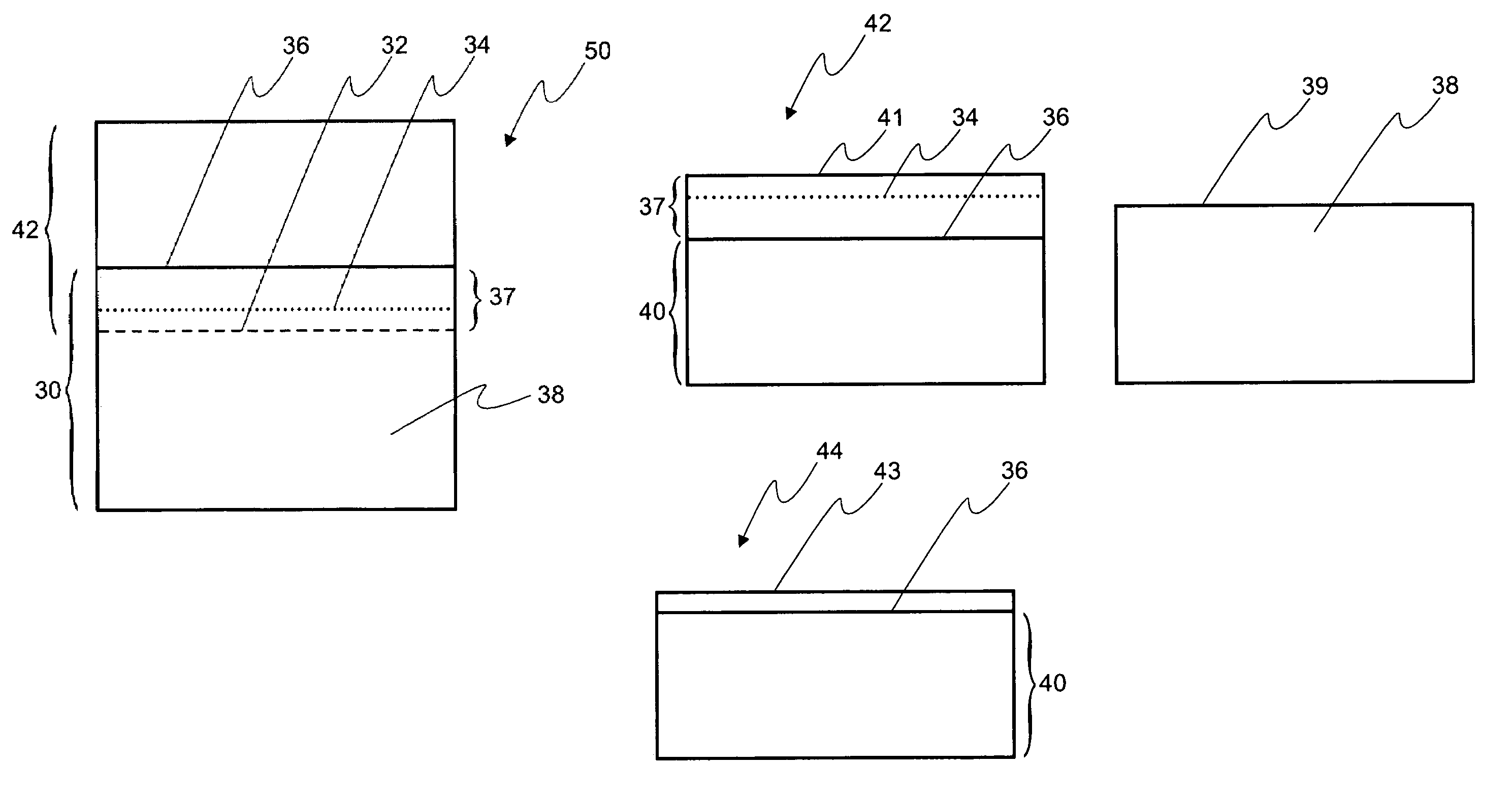
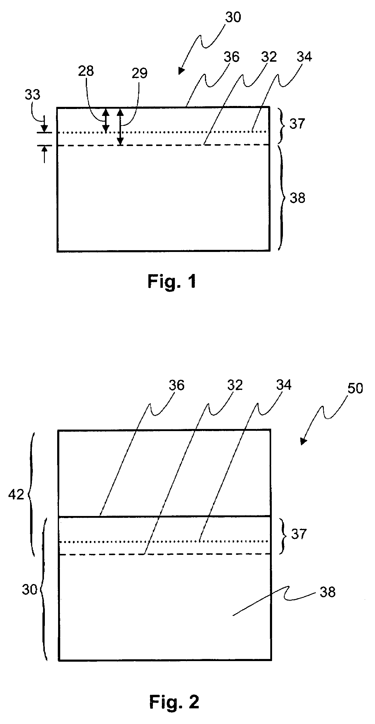
[0053]A first structure S1 and a second structure S2 were produced and compared with respect to the amount of blister formation observed at each respective bonded interface and the resulting surface roughnesses. A region of weakness was formed in the first structure S1 by implanting only a co-implantation of helium and hydrogen species at implantation conditions that typically result in the formation of blisters, i.e., implanting both species at substantially the same depth within the donor substrate and implanting hydrogen species at a relatively low dose. Helium species were implanted with an implantation energy of 49 keV and a dose of 1.5×10¹⁶ / cm2, and hydrogen species were implanted with an implantation energy of 32 keV and a dose of 1×10¹⁶ / cm2.

[0054]The second structure S2 was produced according to a preferred embodiment of the present invention. The implantation of atomic species preferably included an initial co-implantation operation to form a region of weakness in the secon...

example 2

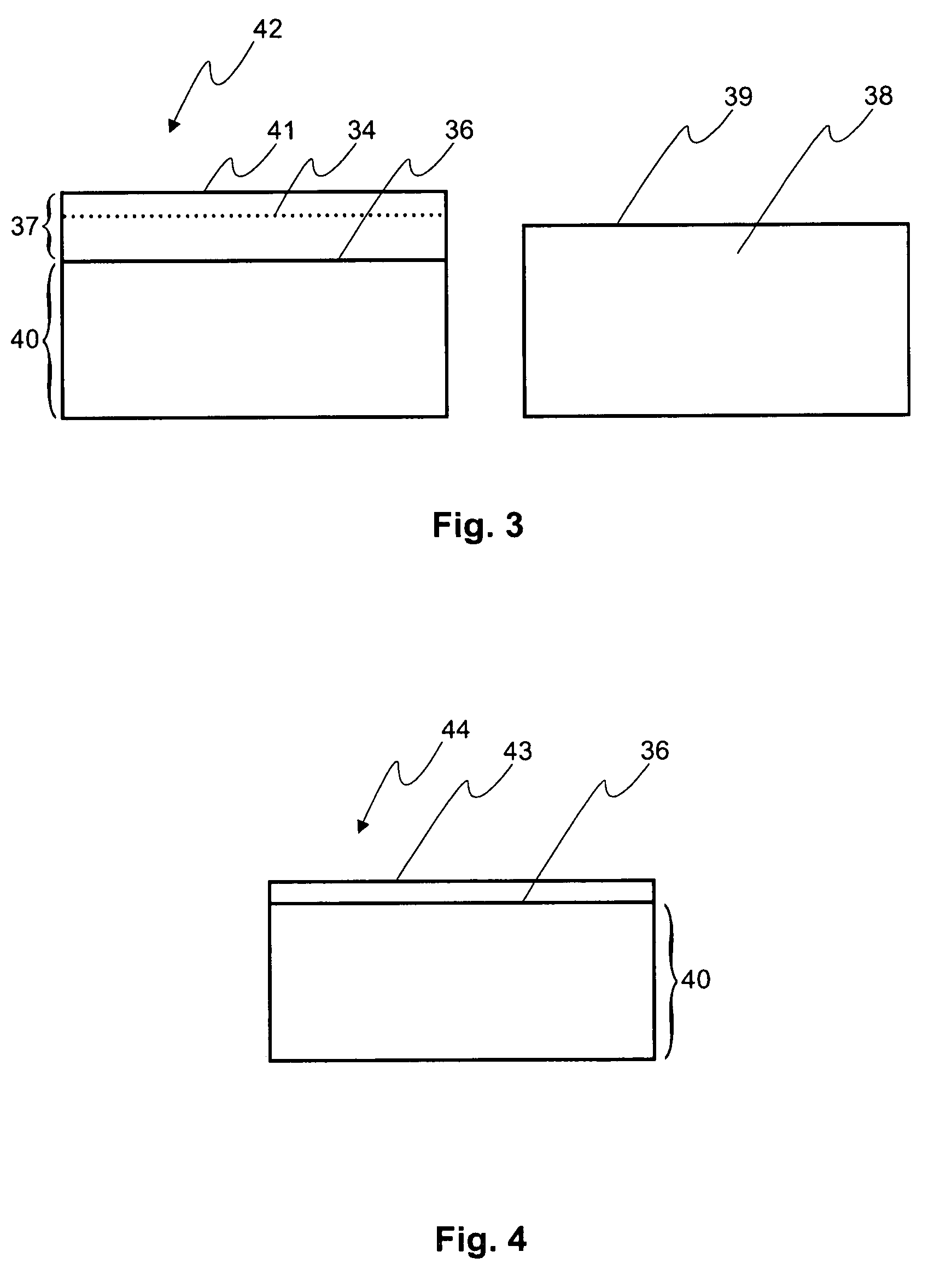
[0060]An SOI structure S3 having a thin layer of buried oxide was produced by oxidizing a silicon substrate to form a superficial oxide layer thereon having a thickness of 200 angstroms. The SOI structure S3 was then subjected to an initial implantation operation of hydrogen species only with an implantation energy of 37 keV and at a dose of 5×10¹⁶ / cm2. A subsequent implantation operation of argon species only was performed with an implantation energy of 200 keV and at a dose of 5×10¹⁴ / cm2.

[0061]Table 2 details the implantation conditions for producing SOI structure S3.

[0062]

TABLE 2S3First implantation operation (H implantation) 37 keV5.1016 / cm2Second implantation operation (Ar implantation)200 keV5.1014 / cm2

[0063]After detachment, very few blisters were observed at the bonded interface of the SOI structure S3, and a 10×10 μm2 AFM scan revealed a surface roughness of about 60 angstroms RMS. The SOI structure S3 was then subjected to an annealing treatment, and a subsequent 10×10 μm2 ...


PUM


Abstract

A method of manufacturing a crystalline wafer that includes implanting first atomic species in a donor substrate to form a region of weakness at a first depth therein and configured to facilitate detachment of a first layer of the donor substrate from a remaining portion of the donor substrate. The first layer and remaining portion are disposed on opposite sides of the region of weakness. The method also includes implanting second atomic species in the donor substrate to form a gettering region at a second depth therein that is different than the first depth to reduce or minimize migration of the implanted first atomic species past the gettering region. This reduces or minimizes an increase in roughness of a surface produced on the first layer after detachment thereof from the remaining portion at the region of weakness.

Description

CROSS-REFERENCE TO RELATED APPLICATIONS[0001]This application is a continuation of International Application PCT / IB2004 / 003301, filed on Sep. 21, 2004, the entire contents of which are expressly incorporated herein by reference thereto.FIELD OF THE INVENTION[0002]The present invention relates generally to a crystalline wafer and a method for manufacturing thereof. More particularly, the method includes forming regions of weakness in a crystalline wafer.BACKGROUND OF THE INVENTION[0003]Several processes and techniques for manufacturing a crystalline wafer by transferring layers are generally known. These include, for example, the layer transfer technique reported in Frontiers of Silicon-on-Insulator, J. Appl. Phys. 93, 4955 (2003) by G. K. Celler et al. and based on the “SMART-CUT®” technology of Soitec S.A., which is known to those skilled in the art and descriptions of which can be found in a number of works dealing with wafer reduction techniques, such as U.S. Pat. No. 5,374,564. ...

Claims


Application Information

Patent Timeline
Patent Type & Authority Patents(United States)
IPC IPC(8): H01L21/46H01L21/30
CPCH01L21/26506H01L21/3223H01L21/76254H01L21/20
Inventor AKATSU, TAKESHI
Owner SOITEC SA
Why Eureka
Try Eureka