Clean process for an electron beam source

a technology of electron beam and electron beam, applied in the direction of chemical vapor deposition coating, manufacturing tools, coatings, etc., can solve the problems of rc delay, power consumption, crosstalk, and increasing complexity of fabrication

Inactive Publication Date: 2008-01-29
APPLIED MATERIALS INC
View PDF12 Cites 10 Cited by
  • Summary
  • Abstract
  • Description
  • Claims
  • Application Information

AI Technical Summary

Problems solved by technology

Fabrication of integrated devices, for example, and without limitation, semiconductor integrated devices, is complicated and, due to increasingly stringent requirements on device designs due to demands for greater device speed, fabrication is becoming ever more complicated.
In the production of advanced integrated circuits that have minimum feature sizes of 0.13 μm and below, problems of RC delay, power consumption, and crosstalk become significant.
Over time, failing to clean the residue from an e-beam treatment apparatus may produce poor process performance, and may also produce high particle counts on wafers that are processed.
This is problematic because it is time consuming, and does not ensure that the chamber is clean.
This is problematic because it is time consuming and because residue is also formed on chamber walls.

Method used


Image

  • Clean process for an electron beam source
  • Clean process for an electron beam source
  • Clean process for an electron beam source

Examples


Embodiment Construction

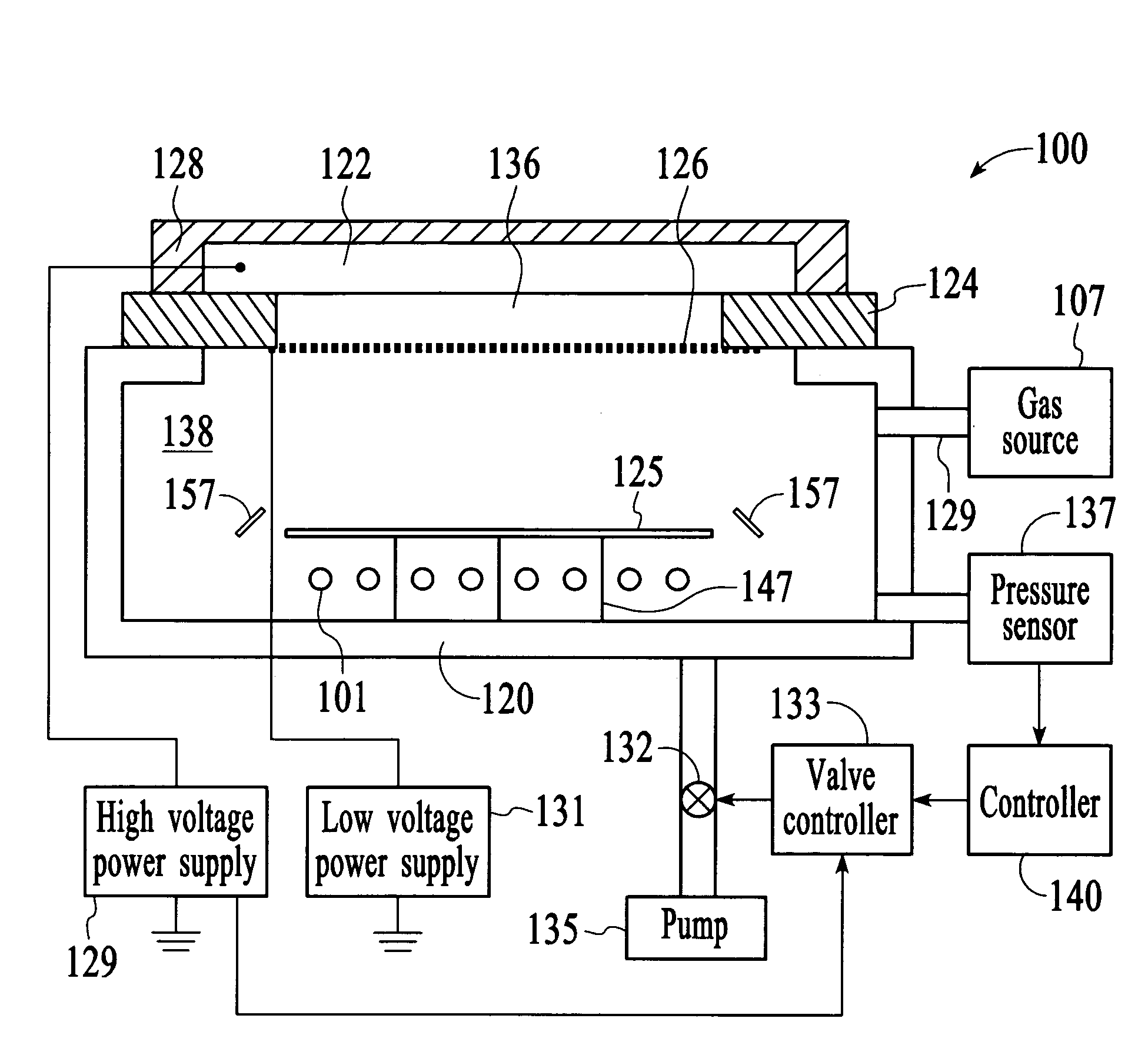
[0014]One or more embodiments of the present invention relate to a method for cleaning an electron beam (e-beam) treatment apparatus such as, for example and without limitation, apparatus 100 shown in FIG. 1.

[0015]FIG. 1 shows a schematic diagram of a partial cross sectional view of large area electron beam source, electron beam treatment apparatus 100 (e-beam apparatus 100) that is available from Applied Materials, Inc. of Santa Clara, Calif. As shown in FIG. 1, e-beam apparatus 100 includes array 101 of quartz halogen lamps for heating a substrate or a wafer, which array is surrounded by heat shield 157 to provide temperature uniformity across a wafer, for example and without limitation, temperature uniformity to within at least 8° C. It should be understood that mechanisms for heating the substrate or wafer are not limited to the use of lamps. In accordance with further embodiments of e-beam apparatus 100, instead of utilizing lamp heating, the wafer or substrate may be disposed ...


PUM

PropertyMeasurementUnit
gas pressureaaaaaaaaaa
currentaaaaaaaaaa
currentaaaaaaaaaa

Abstract

One embodiment of the present invention is a method for cleaning an electron beam treatment apparatus that includes: (a) generating an electron beam that energizes a cleaning gas in a chamber of the electron beam treatment apparatus; (b) monitoring an electron beam current; (c) adjusting a pressure of the cleaning gas to maintain the electron beam current at a substantially constant value; and (d) stopping when a predetermined condition has been reached.

Description

[0001]This is a continuation-in-part of a patent application entitled “Methods and Apparatus for E-Beam Treatment Used to Fabricate Integrated Circuit Devices” having Ser. No. 10 / 428,374 that was filed on May 1, 2003 now issued as U.S. Pat. No. 6,936,551, which patent application claimed the benefit of U.S. Provisional Application No. 60 / 378,799, filed on May 8, 2002, and which patent application is incorporated by reference herein.TECHNICAL FIELD OF THE INVENTION[0002]One or more embodiments of the present invention pertain to apparatus for electron beam treatment used to fabricate integrated circuit devices. In particular, one or more embodiments of the present invention pertain to method and apparatus for cleaning such apparatus.BACKGROUND OF THE INVENTION[0003]Fabrication of integrated devices, for example, and without limitation, semiconductor integrated devices, is complicated and, due to increasingly stringent requirements on device designs due to demands for greater device s...

Claims


Application Information

Patent Timeline
Patent Type & Authority Patents(United States)
IPC IPC(8): H01L21/20B05D3/06B05D7/24C23C16/26C23C16/40C23C16/56H01L21/3105H01L21/312
CPCC23C16/26C23C16/56C23C16/401B05D1/60B05D3/068Y10S438/905H01L21/31058H01L21/76807
Inventor DEMOS, ALEXANDROS T.ELSHEREF, KHALED A.CHANG, JOSPHINE J.M'SAAD, HICHEM
Owner APPLIED MATERIALS INC
Why Eureka
Try Eureka