System and method for multiple cycle capture of chip state

a technology of chip state capture and multiple cycle, applied in the field of very large scale integration (vlsi) testing, can solve the problems of inability to accurately represent the performance characteristics of an actual silicon device, the visibility of the inner state of the vlsi chip has become increasingly limited, and the failure to diagnose failures and measure the performance of state-of-the-art very large scale integration (vlsi) chips

Inactive Publication Date: 2008-01-29
HEWLETT-PACKARD ENTERPRISE DEV LP
View PDF10 Cites 18 Cited by
  • Summary
  • Abstract
  • Description
  • Claims
  • Application Information

AI Technical Summary

Benefits of technology

[0016]The test circuitry may further include a programmable register storing a value corresponding to the predetermined number of cycles. The programmable register selectively increments the value corresponding to the predetermined number of cycles by a predetermined number of the cycles. This feature allows for capturing successive sequences of test data over multiple test runs.

Problems solved by technology

It has become very difficult to diagnose failures in and to measure the performance of state-of-the-art very large scale integration (VLSI) chips.
Moreover, visibility of the VLSI chip's inner state has become increasingly limited due to the complexity of the VLSI chips and to practical constraints on the number of external pads that can be provided on the chip package.
Unfortunately, logic analyzers must rely solely on externally-accessible signals to accomplish this, not on signals that are internal to the chip itself.
But such devices only emulate the functionality of the VLSI chip.
By their very nature, they cannot give an accurate representation of the performance characteristics of an actual silicon device.
These extra pins increase overall costs, and the use of these pins for debug functionality compete with chip functionality resulting in less functionality included within the chip.
Secondly, designing and verifying the software to be used with the logic analyzer or other monitoring device to read and interpret the information obtained from the chip is very costly.
These difficulties result in longer chip debug schedules.
While this solution does reduce the number of pins dedicated to debug operations, several debug port pins are still required in the design and verification of the logic analyzer software is still costly.
Area constraints limit the number of shadow flops that can be placed in the design and the shadow flops tend to be expensive.
So debug operations through the use of shadow registers is limited by the number of shadow flops that can be included in the design and by the difficulty in selecting the most likely places for the shadow flops to be required to provide visibility into the functionality of the chip.
This problem is further exasperated if multiple cycles of information are required for a node or a bus in order to perform debug operations.
While all shadow flops within the chip can be viewed in this manner, if the problem being debugged is not repeatable this process cannot be used.
Typically a large number of scanable flops are included in the chip design and this inclusion results in only a small increase in the area required.
However, in order to perform debug operations in this manner, the clock must be repeatedly halted which interrupts normal operation of the chip during the debug operation.
Additionally, repeatability of the system is still required to debug problems which involve multiple cycles of information.
Because it is serial, this interface is typically limited to providing one bit of test data out for every clock cycle of the unit under test.
Thus, capture of test information is limited.
However, these systems require some compromise between on-chip storage capabilities, pins available for providing signal and data samples, and multiplexing required to provide plural outputs on each available pin.
However, as the circuit under test continues to operate and test results are generated more quickly than the pin count will permit providing thereof, the memory will rapidly continue to fill until, eventually, an overflow condition will be reached, data lost, and circuit operation compromised.

Method used


Image

  • System and method for multiple cycle capture of chip state
  • System and method for multiple cycle capture of chip state
  • System and method for multiple cycle capture of chip state

Examples


Embodiment Construction

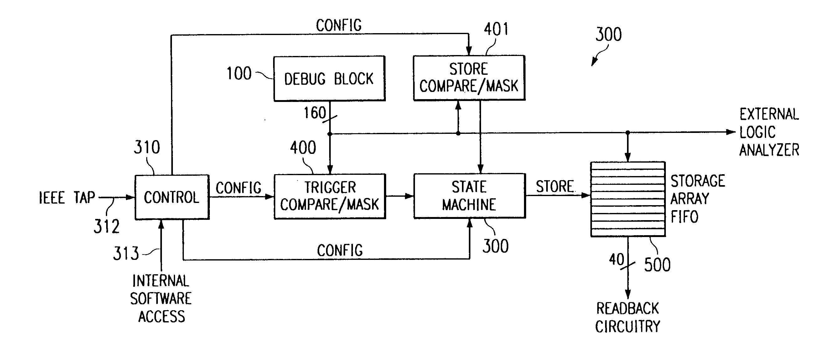
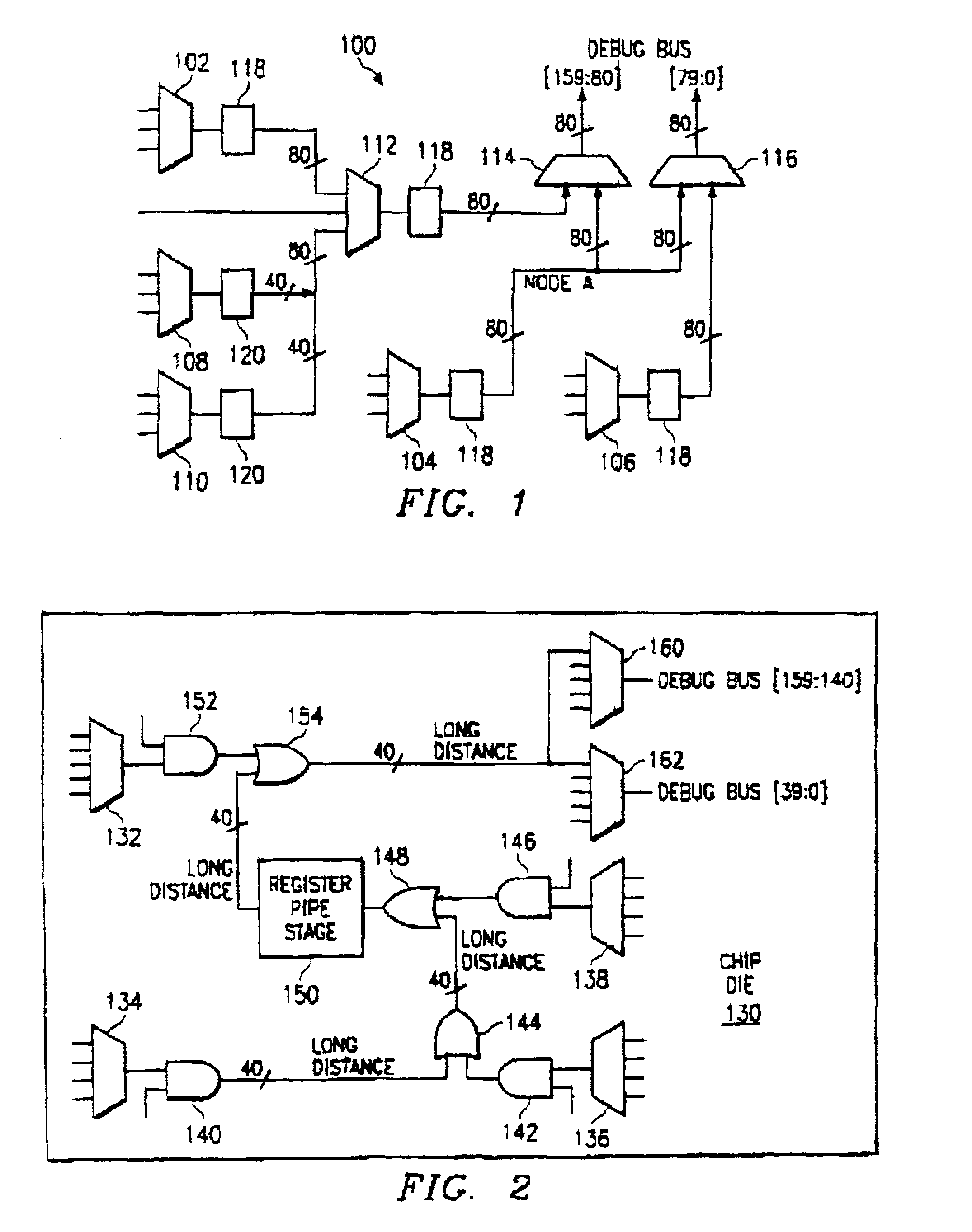
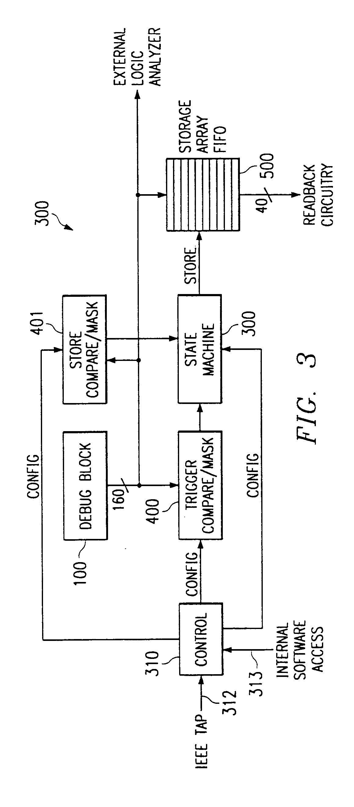
[0040]A preferred embodiment of the invention includes three main components: (1) a debug bus circuit on-chip; (2) flexible trigger / store network; and (3) an on-chip (or off-chip) storage array / FIFO. Each of these components is useful and functional independent of the others but provide additional advantages when combined as here in detail.

[0041]Referring to FIG. 1, an embodiment of the debug bus circuit 100 includes a plurality of multiplexers connected to various sampling points on a chip. The multiplexers may handle various data sample widths. For example, multiplexers 102, 104 and 106 each sample a plurality of 80 bit wide data and / or control signals while multiplexers 108 and 110 each sample up to 40 bits each. While each of the samples may represent a single unit of data such as a data word, the samples may also include various combinations of smaller data units and / or discrete signals collected to provide respective parallel outputs. These outputs may, in turn, combine to pro...


PUM


Abstract

Test circuitry is incorporated on a chip die together with a circuit to be tested, such as an ASIC or microprocessor, to provide external access to signals that are internal to an integrated circuit chip package. A controller provides the arm command and issues appropriate configuration controls to collect signal samples. In particular, a network responds to these commands from the controller to selectively provide signal samples from a device under test. A trigger event generator responds to logic or other characteristics of the signal samples to provide trigger events. These trigger events are counted by a trigger event counter in the armed state of the state machine to identify the final trigger event corresponding to an occurrence of a programmable number of the trigger events. A store event generator also responds to a programmed characteristic or combination(s) of the signal samples to provide a store event. Either or both of the event generators may use a mask to provide these events.

Description

TECHNICAL FIELD [0001]This invention relates generally to very large scale integration (VLSI) testing, and more particulary to a system and method for on-chip debug support and performance monitoring for microprocessors and microprocessor systems.BACKGROUND[0002]It has become very difficult to diagnose failures in and to measure the performance of state-of-the-art very large scale integration (VLSI) chips. This is because modern VLSI chips often not only run at very high clock speeds, but many of them also execute instructions in parallel, out of program order and speculatively. Moreover, visibility of the VLSI chip's inner state has become increasingly limited due to the complexity of the VLSI chips and to practical constraints on the number of external pads that can be provided on the chip package.[0003]In the past, the traditional failure diagnosis and performance measurement tools have been external logic analyzers and in-circuit emulators. Logic analyzers are capable of monitor...

Claims


Application Information

Patent Timeline
Patent Type & Authority Patents(United States)
IPC IPC(8): G06F11/00G01R31/3185
CPCG01R31/318522
Inventor SWANSON, JEFFREY C.EBNER, SHARON M.WICKERAAD, JOHN A.
Owner HEWLETT-PACKARD ENTERPRISE DEV LP
Why Eureka
Try Eureka