Assembly of semiconductor device, interposer and substrate
a technology of interposer and semiconductor device, which is applied in the direction of fixed capacitor details, fixed capacitors, printed circuit non-printed electric components association, etc., can solve the problems of increasing the loss, and difficult to manufacture the assembly at low cost. , to achieve the effect of enhancing the ability of removing noise, increasing the length of capacitor connecting wiring, and reducing the loss
- Summary
- Abstract
- Description
- Claims
- Application Information
AI Technical Summary
Benefits of technology
Problems solved by technology
Method used
Image

Examples
first embodiment
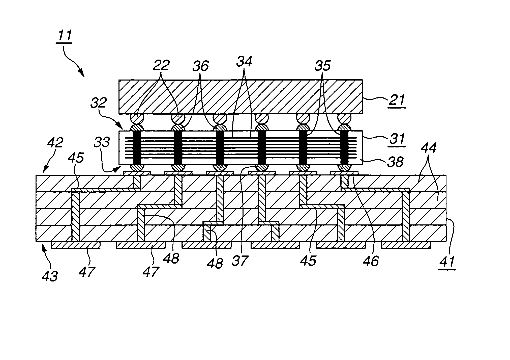
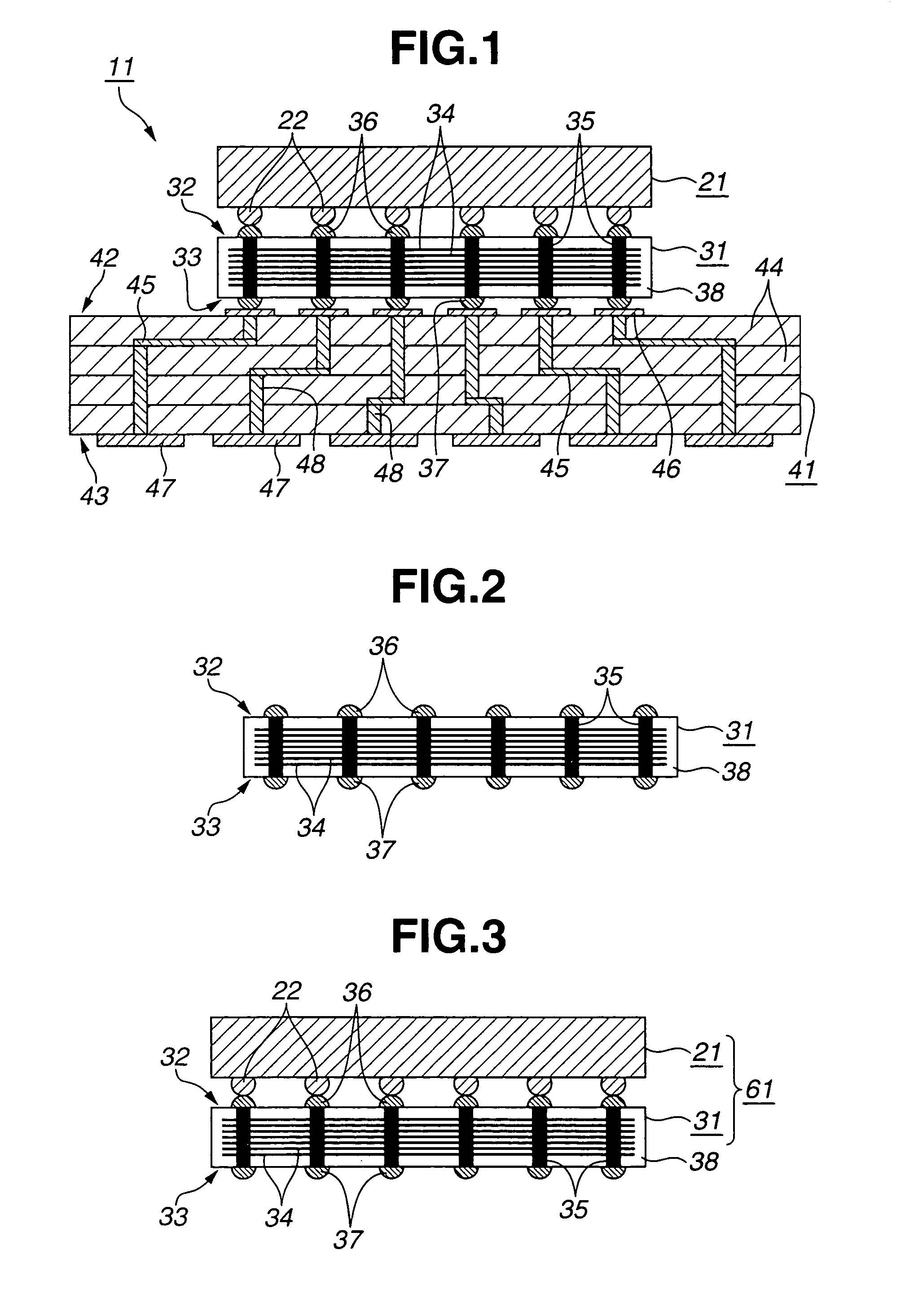
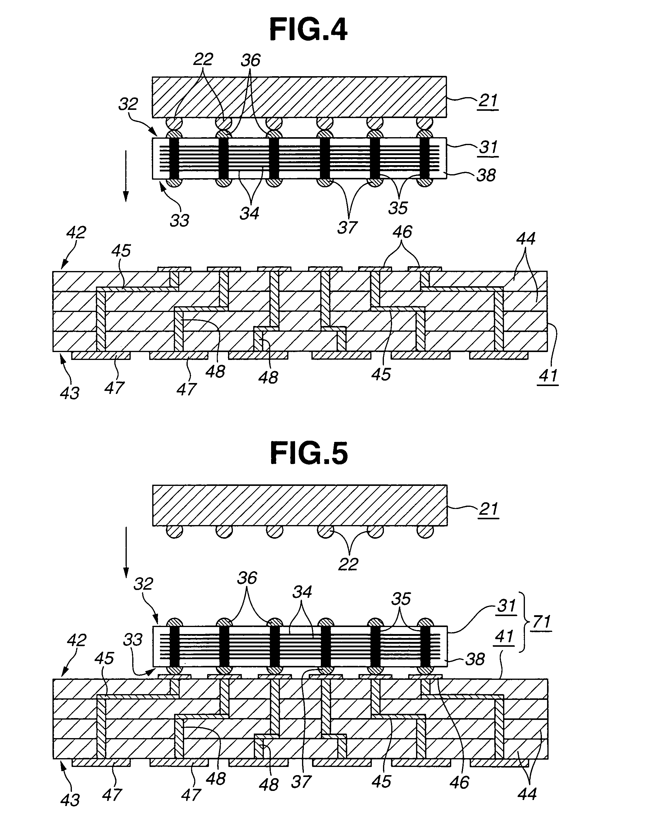
[0092]Referring first to FIGS. 1 and 5, a semiconductor package (an assembly of a semiconductor device, a capacitor and a substrate) according to a first embodiment of the present invention is generally indicated by 11 and of the LGA (land grid array) type including an IC chip (semiconductor device) 21, a capacitor 31 and a circuit substrate (substrate) 41. In the meantime, the semiconductor package 11 is not limited to the LGA type but can be of any other type such as BGA (ball grid array) type and PGA (pin grid array) type. The IC chip 21 having a function of MPU (micro processing unit) is in the form of a flat plate of 10 mm square and made of silicon of thermal expansion coefficient of about 3.0 ppm / ° C. On the upper side surface of the IC chip 21 is formed a circuit element (not shown). On the other hand, on the lower side surface of the IC chip 21 is formed a plurality of surface-connecting terminals 22 in the form of bumps.
[0093]The circuit substrate 41 is in the form of a sq...
second embodiment
[0109]Referring to FIGS. 6 to 10, a semiconductor package (an assembly of a semiconductor device, an interposer and a substrate) according to a second embodiment of the present invention will be described. In FIG. 6, the semiconductor package is generally indicated by 131 and includes an IC chip (semiconductor device) 21, a capacitor built-in interposer (capacitor equipped interposer assembly) 91 and a circuit substrate (substrate) 41.
[0110]As shown in FIG. 6, the semiconductor package 131 of this embodiment is of the LGA (land grid array) type including, as described above, the IC chip 21, a capacitor built-in interposer 91 and the circuit substrate 41. In the meantime, the semiconductor package 131 is not limited to the LGA type but can be of another type such as BGA (ball grid array) and PGA (pin grid array). The IC chip 21 and the circuit substrate 41 are the same as those utilized in the first embodiment, so that detailed description thereto is omitted.
[0111]As shown in FIGS. 6...
third embodiment
[0138]Referring to FIG. 13, a semiconductor package (an assembly of a semiconductor device, an interposer and a substrate) according to a third embodiment of the present invention is generally indicated by 181 and includes an IC chip (semiconductor device) 21, capacitor built-in interposer 151 and a circuit substrate (substrate) 41.
[0139]The capacitor built-in interposer 151 in this embodiment includes a plurality of interposer side electrically conductive ground vias 182 and a plurality of interposer side electrically conductive power vias 183. Both of the two kinds of interposer side electrically conductive vias 182, 183 are disposed within a recess forming area of the interposer main body 98. Within the recess forming area are similarly disposed a plurality of short electrically conductive ground vias 188 and a plurality of short electrically conductive power vias 189. On the other hand, a plurality of interposer main body side electrically conductive vias 184 for signal lines ar...
PUM
 Abstract
Description
Claims
Application Information
 - R&D
- Intellectual Property
- Life Sciences
- Materials
- Tech Scout
- Unparalleled Data Quality
- Higher Quality Content
- 60% Fewer Hallucinations
Browse by: Latest US Patents, China's latest patents, Technical Efficacy Thesaurus, Application Domain, Technology Topic, Popular Technical Reports.
© 2025 PatSnap. All rights reserved.Legal|Privacy policy|Modern Slavery Act Transparency Statement|Sitemap|About US| Contact US: help@patsnap.com