Low dielectric semiconductor device and process for fabricating the same

a low-dielectric semiconductor and semiconductor technology, applied in semiconductor devices, semiconductor/solid-state device details, electrical apparatus, etc., can solve the problems that porous ultra-low dielectric constant materials cannot survive standard wafer processing without failure or delimitation of high-modulus dielectric materials, and achieve low cost and high resolution

Inactive Publication Date: 2008-02-12
GOOGLE LLC
View PDF5 Cites 1 Cited by
  • Summary
  • Abstract
  • Description
  • Claims
  • Application Information

AI Technical Summary

Benefits of technology

[0011]Accordingly, it is an object of the present invention to provide a method for achieving a low K chip interconnect structure that circumvents the problems and limitations described above.
[0013]It is another object of this invention to provide a practical, low cost and high resolution solution for the integration of ultra low K dielectric materials by adapting a contact printing technique, which does not require the conventional fabrication steps of patterning, etching or alignment, addresses issues in the science of manufacturing at scales below 200 nm, and allows new approaches to fabrication of assembling devices.
[0014]It is yet another object of the present invention to provide a support structure for porous ultra low dielectric constant materials formed of an insulating material that enables the porous ultra low dielectric constant material to sustain mechanical stress during chemical-mechanical polishing processing.
[0015]It is a further object of the present invention to provide a process in which the area ratio of support structure to porous low dielectric constant material is very low, such that the overall dialectic constant of the combination remains close to that of the porous low dielectric constant material.

Problems solved by technology

Use of porous ultra low dielectric constant materials in high performance microelectronic device chips, while desirable, is problematic due to their porosity and poor mechanical stability.
Porous ultra low dielectric constant materials cannot survive standard wafer processing without failure or delimitation of the high modulus dielectric material.

Method used


Image

  • Low dielectric semiconductor device and process for fabricating the same
  • Low dielectric semiconductor device and process for fabricating the same
  • Low dielectric semiconductor device and process for fabricating the same

Examples


Embodiment Construction

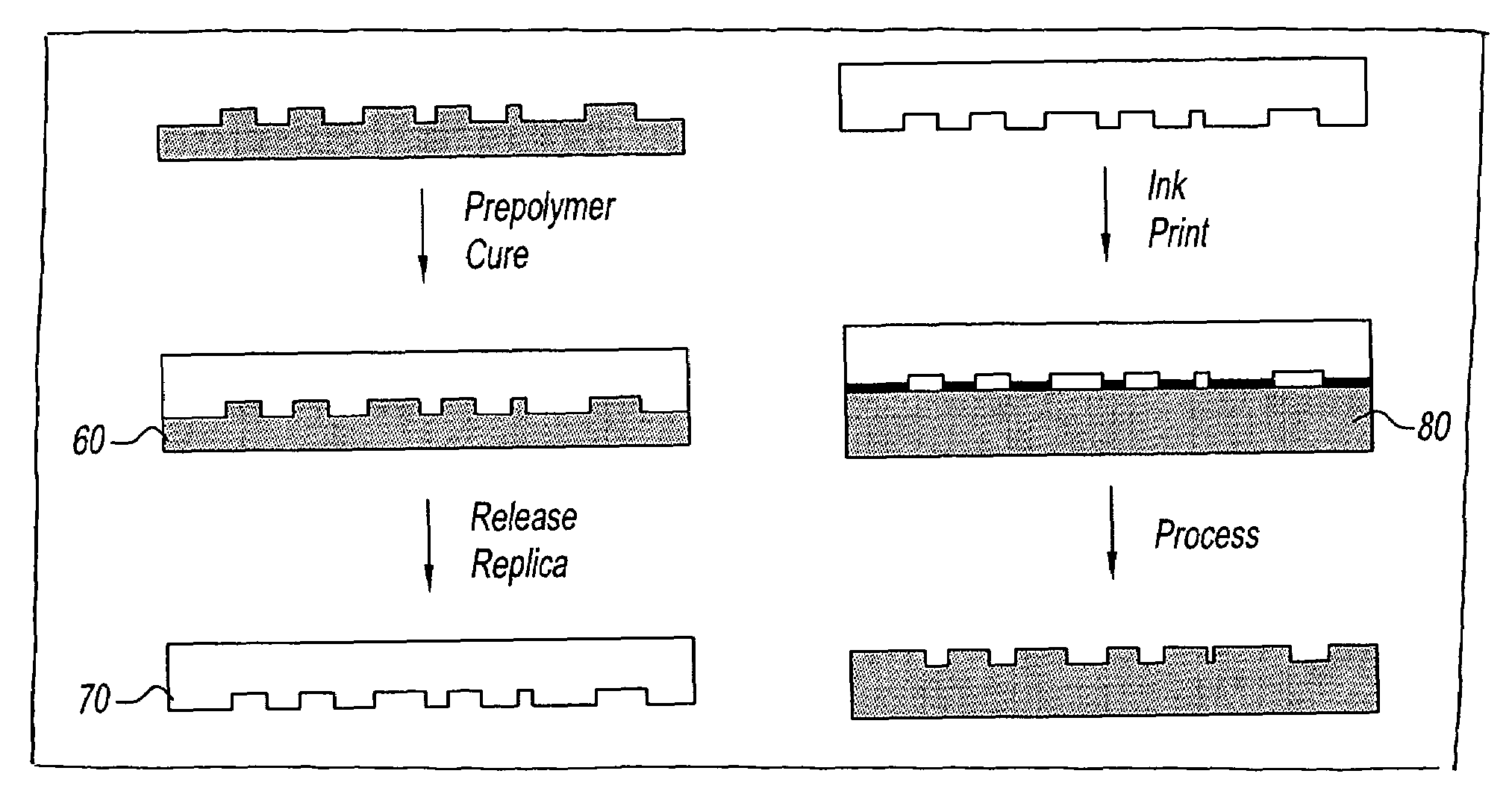
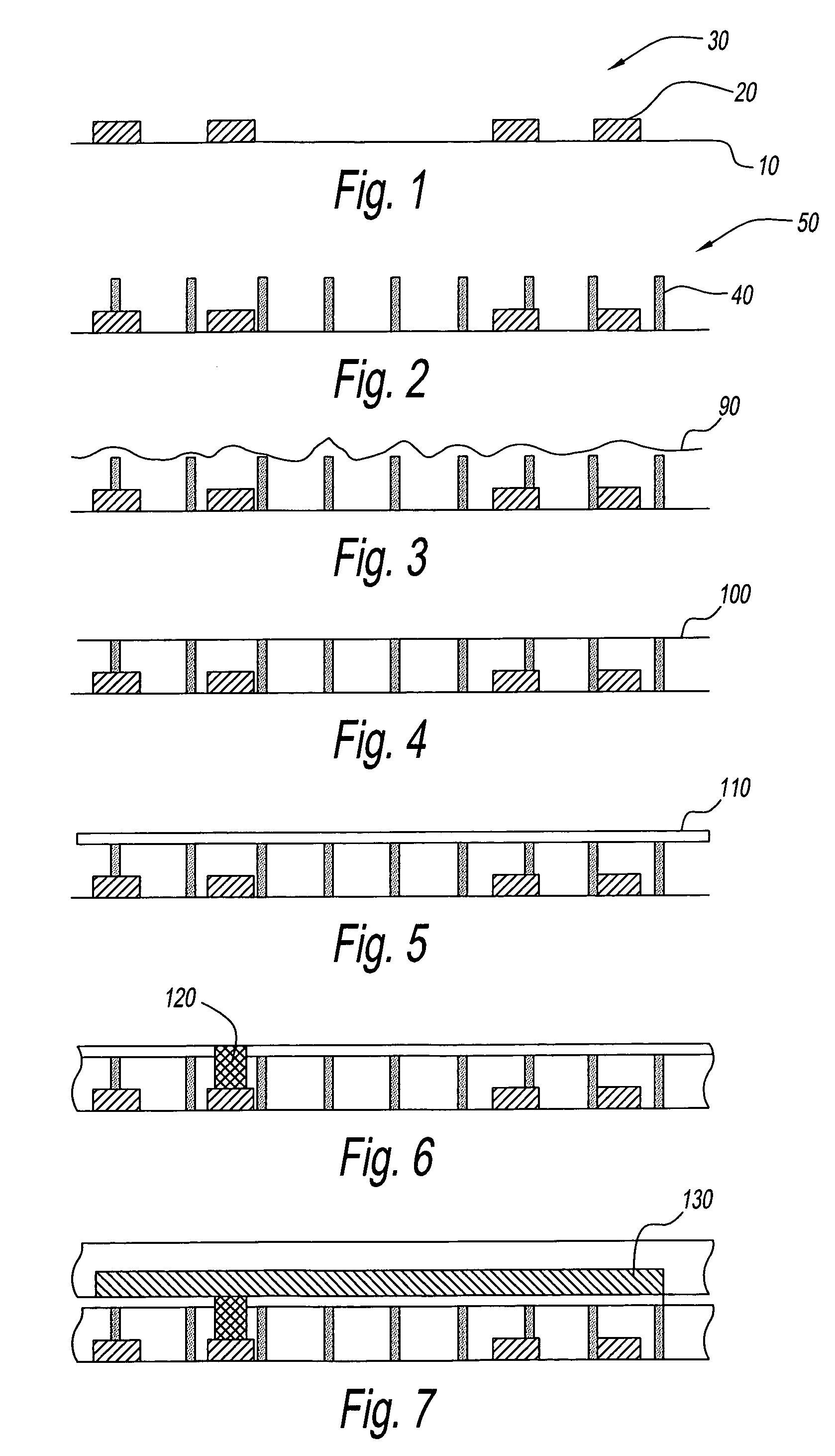
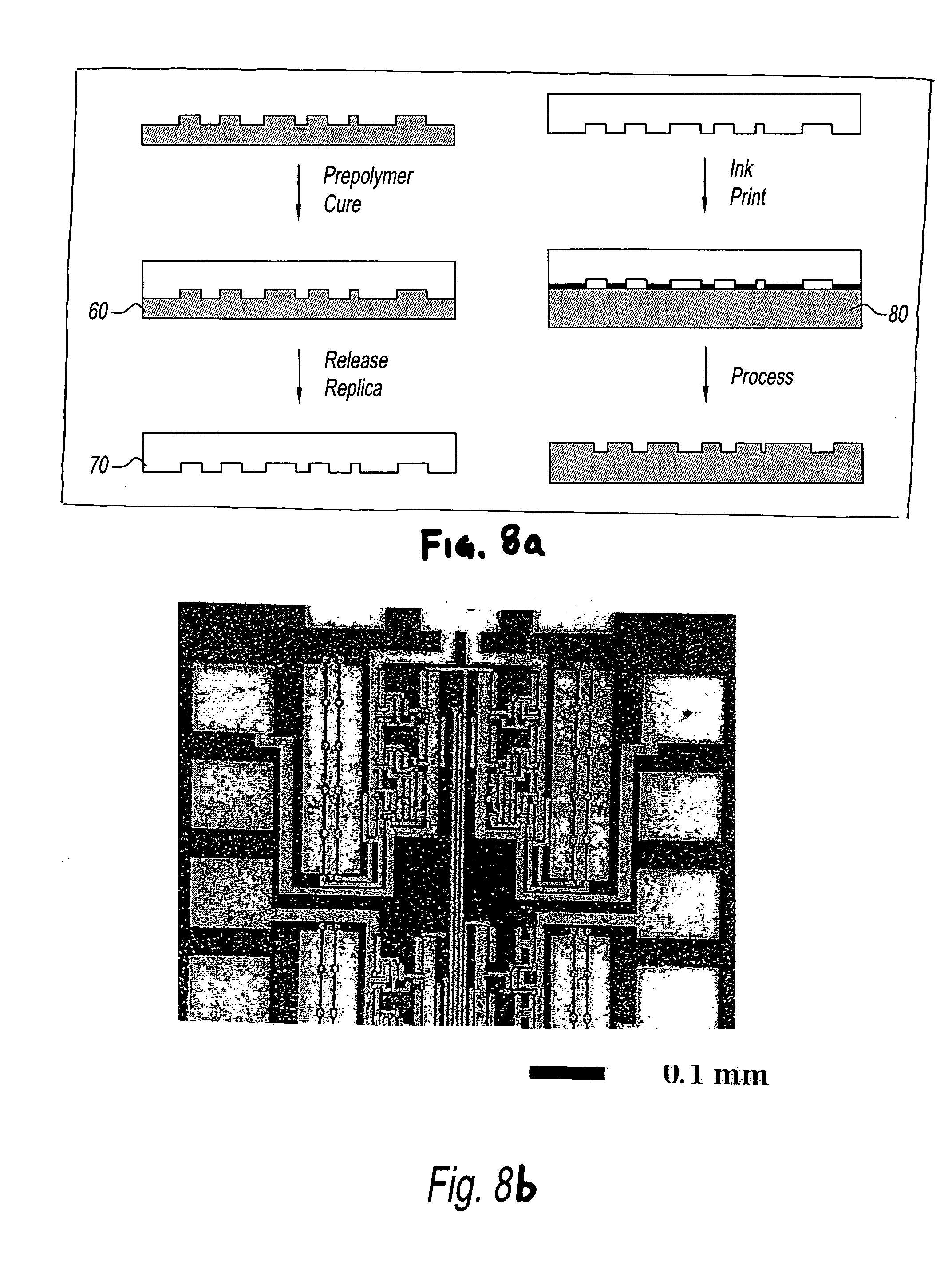
[0028]The present invention discloses a process for fabricating a multilayer low dielectric K semiconductor device that possesses a very low capacitance and, hence, fast propagation speeds. The semiconductor of the present invention successfully integrates a porous, and therefore brittle, ultra low K dielectric insulating material (or materials) by employing a non-porous low K dielectric insulating material support structure. The support structure acts as a support, which enables the ultra low K dielectric to sustain mechanical stresses applied during the chemical-mechanical polishing steps. The semiconductor device is formed by the following sequence:

[0029]A first metal layer 20 is deposited on a substrate 10, as illustrated in FIG. 1. First metal layer 20 may be formed of aluminum, copper or similar material. First metal layer 20 is patterned to produce a patterned first metal wiring 30. Patterning of first metal layer 20 is accomplished by conventional methods known in the art su...


PUM

PropertyMeasurementUnit
dielectric constantaaaaaaaaaa

Abstract

A process for fabricating a low dielectric constant semiconductor comprising the steps of: depositing a first metal layer on a substrate; patterning the first metal layer to produce a patterned first metal wiring; applying a first insulating material onto the patterned first metal wiring to form a support structure; patterning the first insulating material by a contact printing process; depositing a second insulating material of lower dielectric constant onto the support structure; planarizing the second insulating material; depositing a polish-stop film layer over the planarized second insulating material, thereby forming a plurality of metal studs; depositing a second metal layer onto the polish-stop film layer forming interconnects with said studs; and patterning the metal layer to produce a second metal wiring interconnecting to the first wiring via the metal studs.

Description

BACKGROUND OF THE INVENTION[0001]1. Field of the Invention[0002]This invention pertains to the field of microelectronic chip fabrication for logic, memory, communication and microcontroller applications. More particularly, this application pertains to the use of a support structures to enable the integration of ultra low dielectric constant (K) materials in semiconductor devices.[0003]2. Description of the Prior Art[0004]The operating speeds of silicon integrated circuits are increasing at phenomenal rates to meet aggressive performance demands in computing, communication and microcontroller applications. This in turn necessitates that signal propagation delays in the wiring that is used to interconnect the circuits on a chip be reduced so that performance is not unduly limited or hampered by interconnect delays. Interconnect delays in chips occur due to the RC time constants wherein R is the resistance of the on chip wiring and C is the effective capacitance between the signal line...

Claims


Application Information

Patent Timeline
Patent Type & Authority Patents(United States)
IPC IPC(8): H01L21/4763H01L21/31H01L21/768H01L23/52H01L23/522H01L23/532
CPCH01L21/76829H01L21/76835H01L23/5222H01L23/53295H01L2924/0002H01L2924/00
Inventor CLEVENGER, LAWRENCEHSU, LOUISTYBERG, CHRISTY S.YUAN, TSORNG-DIH
Owner GOOGLE LLC
Why Eureka
Try Eureka