

Circuit device and manufacturing method thereof
a manufacturing method and circuit device technology, applied in the direction of printed element electric connection formation, association of printed circuit non-printed electric components, non-metallic protective coating application, etc., can solve the problems of increasing the size of the entire circuit device, high-precision and expensive exposure machine or laser irradiator, and reducing the reliability of the adhesive against thermal stress. , curtailing the formation of conventional exposed portions, enhancing the positional accuracy of the conductive pattern
- Summary
- Abstract
- Description
- Claims
- Application Information
AI Technical Summary
Benefits of technology
Problems solved by technology
Method used
Image

Examples
first embodiment
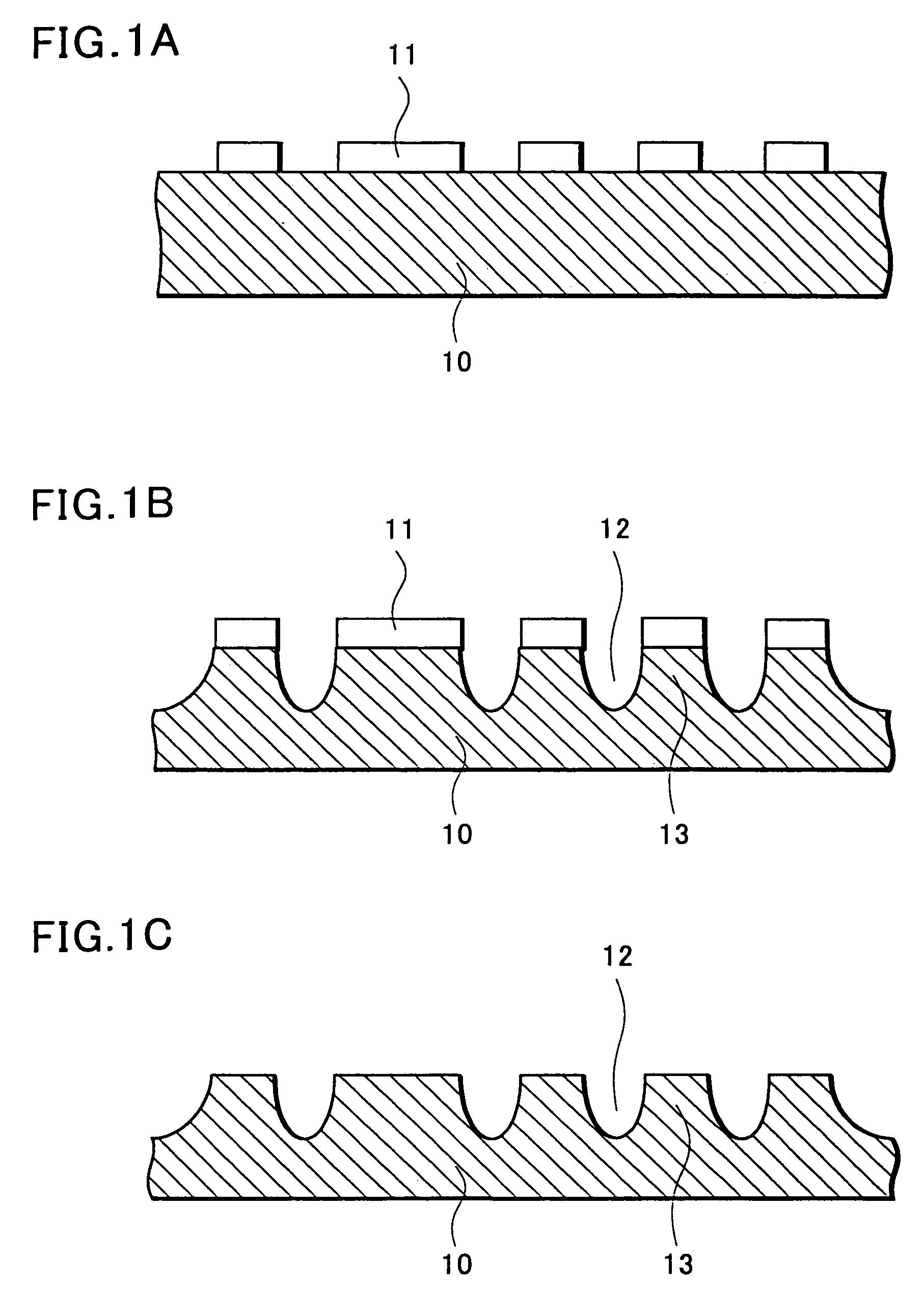
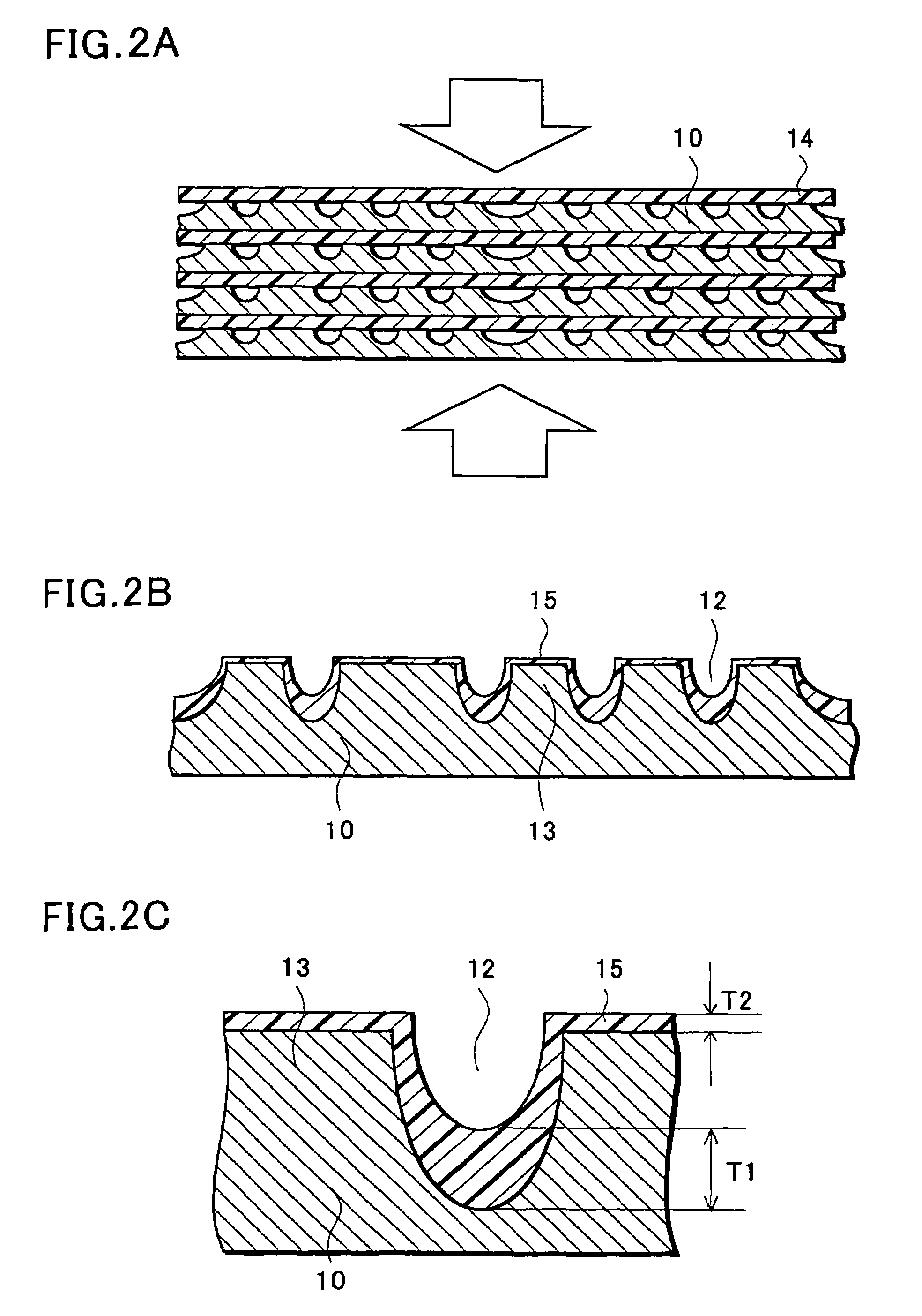
[0043]A method of manufacturing a circuit device according to a first embodiment will be described with reference to FIG. 1A to FIG. 5C. The method of manufacturing a circuit device of this embodiment includes the steps of preparing conductive foil 10, forming conductive patterns 13 in convex shapes by forming isolation trenches 12 on a surface of the conductive foil 10, covering the surface of the conductive foil 10 with resin film 15 so as to form the resin film 15 covering the isolation trenches 12 thicker than the resin film 15 covering upper surfaces of the conductive patterns 13, exposing the upper surfaces of the conductive patterns 13 out of the resin film 15 by removing the resin film 15, electrically connecting the conductive patterns 13 exposed out of the resin film 15 to circuit elements, forming sealing resin 20 to seal the circuit elements, and removing a rear surface of the conductive foil 10 until the conductive patterns 13 are mutually isolated. In the following, a ...
second embodiment
[0064]In this embodiment, a method of manufacturing a circuit device in the case of adopting a face-down semiconductor element as an embedded circuit element will be described with reference to FIG. 6A to FIG. 7C. Basic points of the method of manufacturing a circuit device of this embodiment are similar to the above-described first embodiment. Accordingly, description will be made below mainly on different points.
[0065]Firstly, as shown in FIG. 6A and FIG. 6B, conductive patterns 13 are formed into convex shapes by forming isolation trenches 12 on a surface of conductive foil 10. Here, the conductive patterns 13 are mainly formed for the purpose of connecting pads for an element to be disposed in a face-down manner. After completing formation of the isolation trenches 12, etching resist 11 is peeled off.
[0066]Next, as shown in FIG. 6C, resin film 15 is formed on the surface of the conductive foil 10, and then upper surfaces of the conductive patterns 13 are exposed out of the resin...
third embodiment
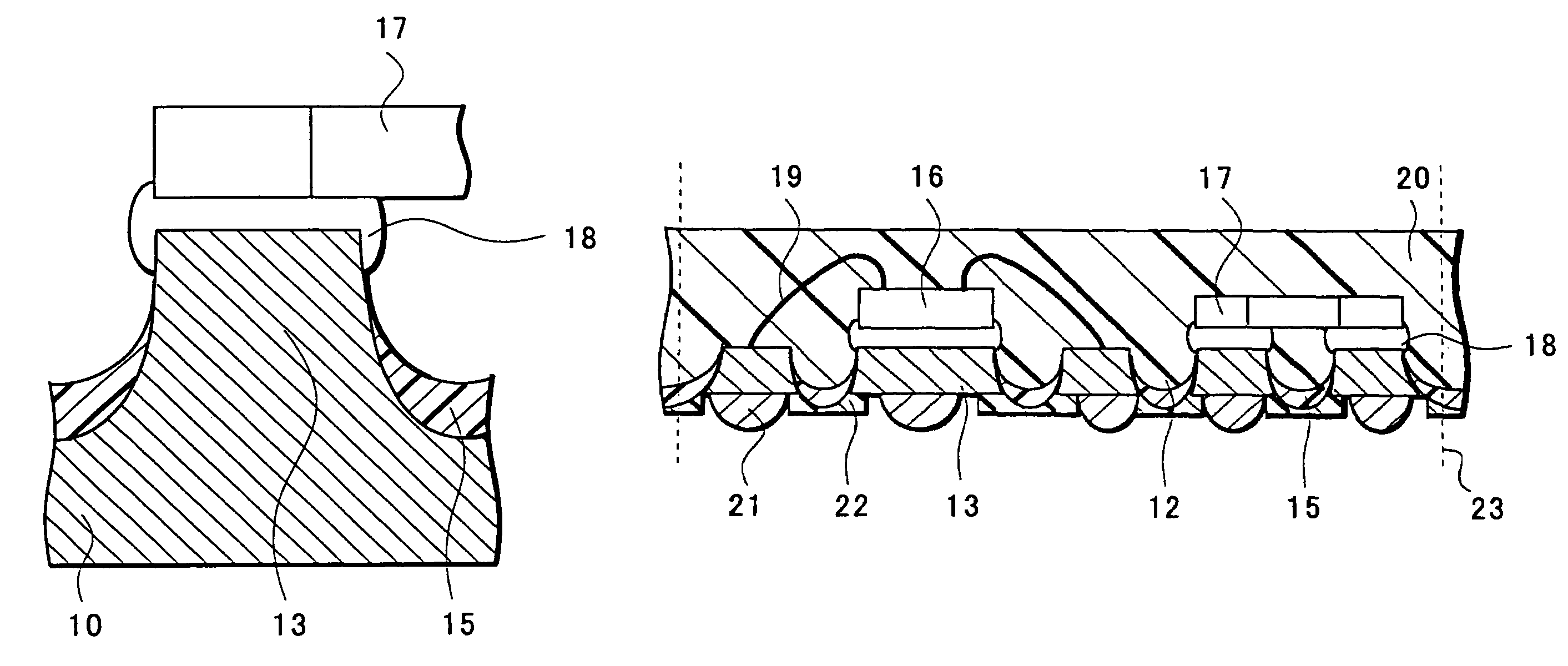
[0070]This embodiment will describe one example of the circuit device which can be manufactured by the above-described embodiments. FIG. 8A is a plan view of circuit device 9, and FIG. 8B is a cross-sectional view thereof. The circuit device 9 shown in these drawings embeds a plurality of circuit elements, and the respective circuit elements are electrically connected to one another through metal thin lines 19 or conductive patterns 13.
[0071]A planar shape of the conductive patterns 13 will be further described with reference to FIG. 8A. In this drawing, upper surfaces 13A of the conductive patterns are indicated by solid lines and lower surfaces 13B of the conductive patterns are indicated by dashed lines. Each upper surface 13A of the conductive pattern constitutes a die pad region where a circuit element is mounted and a bonding pad region where a metal thin line is connected. As described previously, the conductive patterns 13 in this specification have very high positional accu...
PUM
 Abstract
Description
Claims
Application Information