Electroplating tool for semiconductor manufacture having electric field control

Active Publication Date: 2008-02-19
BELL SEMICON LLC
View PDF6 Cites 26 Cited by
  • Summary
  • Abstract
  • Description
  • Claims
  • Application Information

AI Technical Summary

Benefits of technology

[0014]The subject invention provides the ability to modify, improve and/or modulate the electromagnetic field lines (field) produced by the electroplating process (i.e. the electroplating circuit). In general, this provides improvement in the uniformity of metal deposition on the semiconductor wafer. This is particularly seen at the edge areas of the semiconductor wafer.
[0015]The subject invention allows an electroplating tool to meet the uniformity needs of the post plat

Problems solved by technology

As semiconductor technology advances, the complexity of integrated circuits increases.
This increased complexity typically results in smaller integrated circuit elements.
While such existing approaches to the control of electroplating of semiconductor devices provide relatively good cont

Method used


Image

  • Electroplating tool for semiconductor manufacture having electric field control
  • Electroplating tool for semiconductor manufacture having electric field control
  • Electroplating tool for semiconductor manufacture having electric field control

Examples


Embodiment Construction

)

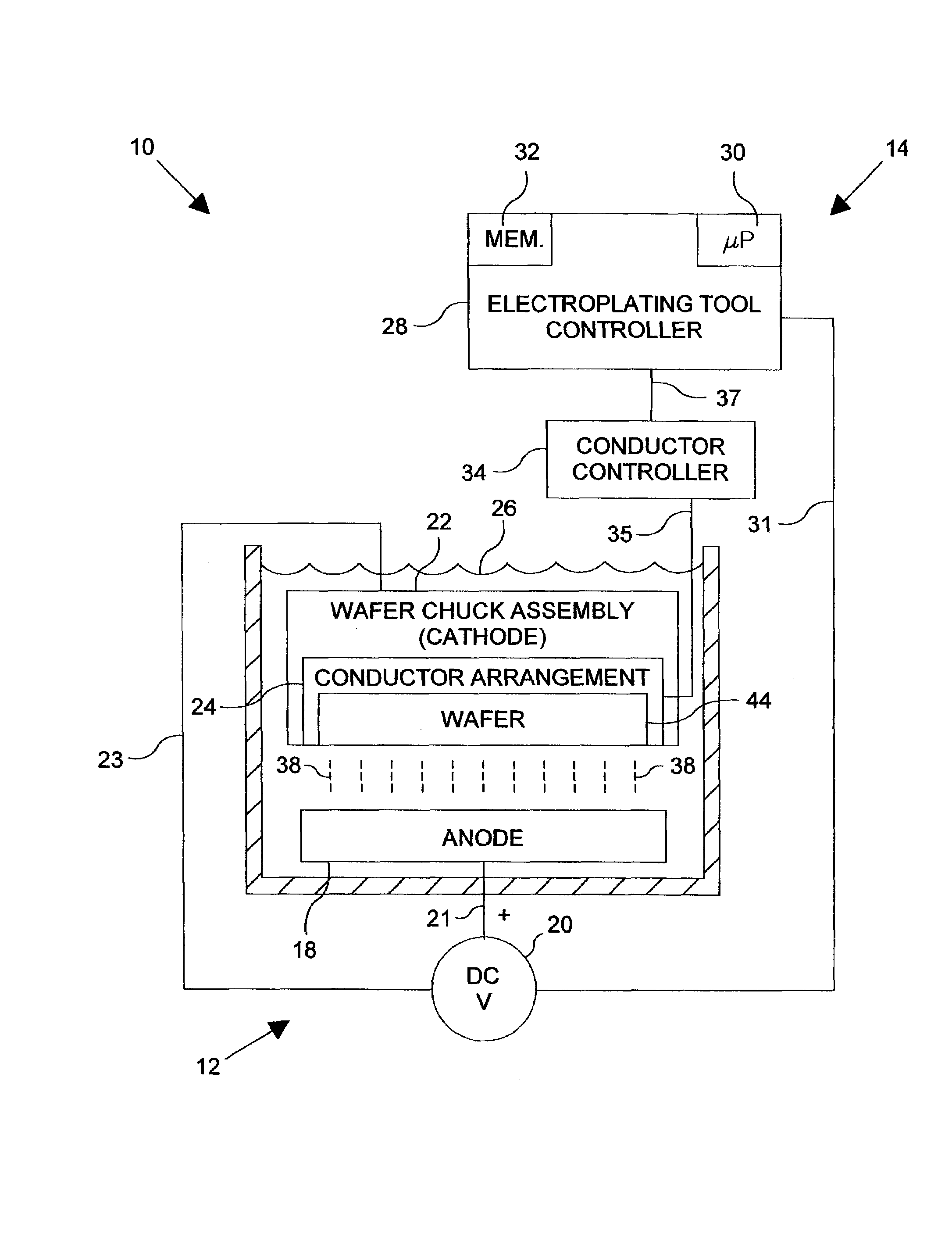
[0021]With reference now to FIG. 1, there is shown a representation of an exemplary electroplating system generally designated 10 in which the subject invention is incorporated and / or is a part thereof. The electroplating system 10 includes an electroplating tool 12 that is coupled to an electroplating control system 14. In general, the electroplating tool 12 is operative, configured and / or adapted to apply, form, deposit or the like, a metal, such as copper, onto a workpiece, such as a semiconductor wafer. The electroplating tool 12 uses the process of electroplating to accomplish the application of the metal. It should be understood that while the subject electroplating tool 12 may be used to provide the electroplating of various metals onto a semiconductor wafer for fabrication or manufacture of various components or elements of integrated circuits, the subject invention will be discussed with respect to the electroplating of the metal copper for interconnects of an integrated c...


PUM

PropertyMeasurementUnit
Electric fieldaaaaaaaaaa
Electrostatic fieldaaaaaaaaaa
Electromagnetic fieldaaaaaaaaaa

Abstract

An electroplating tool for providing a metal or metal film on a semiconductor wafer during processing thereof has a wafer chucking mechanism with a conductor or conductors associated therewith. The conductor(s) are electrically connected to a controller that applies a voltage or current applied thereto for altering the position of and/or varying the intensity of electromagnetic field lines originating from a source anode of the electroplating tool. The electromagnetic field lines originating from the source anode direct the deposition of metal from the electroplating solution to the semiconductor wafer. The conductor(s) of the wafer chucking mechanism improve and/or modulate the electromagnetic field lines of the electroplating process. This provides greater control of metal deposition during the electroplating process such that uniformity of the metal (e.g. copper) is provided across the semiconductor wafer.

Description

BACKGROUND[0001]1. Field of the Invention[0002]The subject invention relates generally to electroplating systems for semiconductor technology and, more specifically, to an electroplating tool for semiconductor devices having electric field control.[0003]2. Background Information[0004]Semiconductor devices such as integrated circuits (ICs) form at least part of almost every electronic product. As semiconductor technology advances, the complexity of integrated circuits increases. This increased complexity typically results in smaller integrated circuit elements. Because of the decrease in size of the circuit elements, the techniques for producing the circuit elements, and thus the integrated circuit itself, need to be quite precise.[0005]The manufacture of semiconductor devices involves many steps and processes. Some processes are utilized several times during the manufacture of a semiconductor device. There are many steps in the manufacture of semiconductor devices that require elect...

Claims


Application Information

Patent Timeline
IPC IPC(8): C25D17/00C25D17/06C25D7/12
CPCC25D17/06C25D17/001C25D17/005
Inventor REDER, STEVEN E.BERMAN, MICHAEL J.
Owner BELL SEMICON LLC
Why Eureka
Try Eureka