Metal gate transistors with epitaxial source and drain regions

a metal gate transistor and drain region technology, applied in the field ofmos transistors, can solve the problems of deteriorating the performance of the transistor, requiring relative high temperature processing,

Active Publication Date: 2008-02-19
TAHOE RES LTD
View PDF10 Cites 144 Cited by
  • Summary
  • Abstract
  • Description
  • Claims
  • Application Information

AI Technical Summary

Problems solved by technology

One problem that occurs, however, is that when the gate structures are formed, relatively high temperature processing is needed to, for instance, activate the doping in a polysilicon gate.
This causes the diffusion of the dopant from the substrate into the channel region, thereby deteriorating the performance of the transistors.

Method used


Image

  • Metal gate transistors with epitaxial source and drain regions
  • Metal gate transistors with epitaxial source and drain regions
  • Metal gate transistors with epitaxial source and drain regions

Examples


Embodiment Construction

[0021]A process for fabricating complementary metal-oxide-semiconductor (MOS) field-effect transistors and the resultant transistors are described. In the following description, numerous specific details are set forth such as specific dopant concentration levels, specific chemicals, etc. in order to provide a thorough understanding of the present invention. It will be apparent to one skilled in the art that these specific details are not required to practice the present invention. In other instances, well-known processing steps, such as cleaning steps, are not described in detail in order not to unnecessarily obscure the following disclosure.

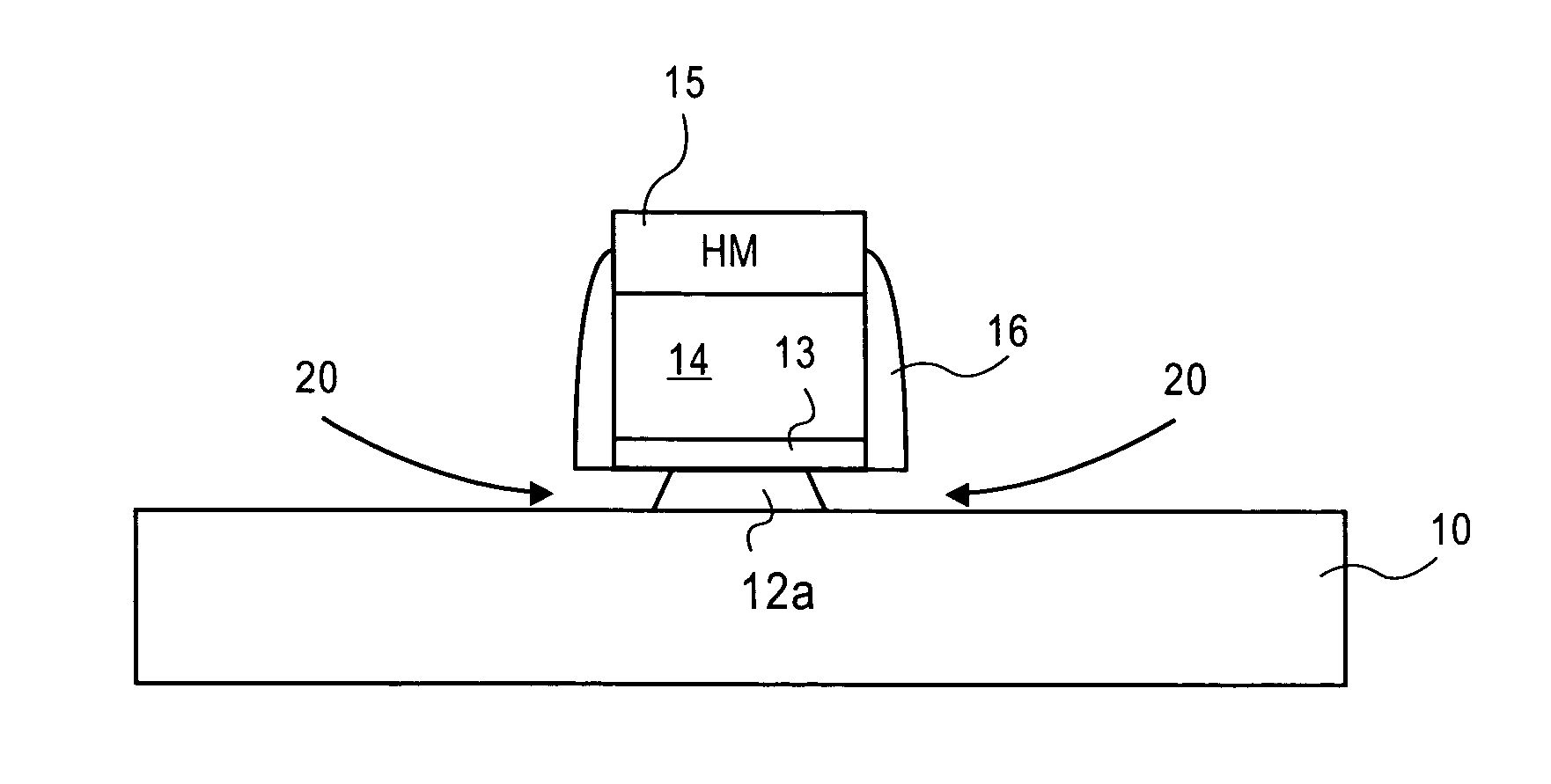
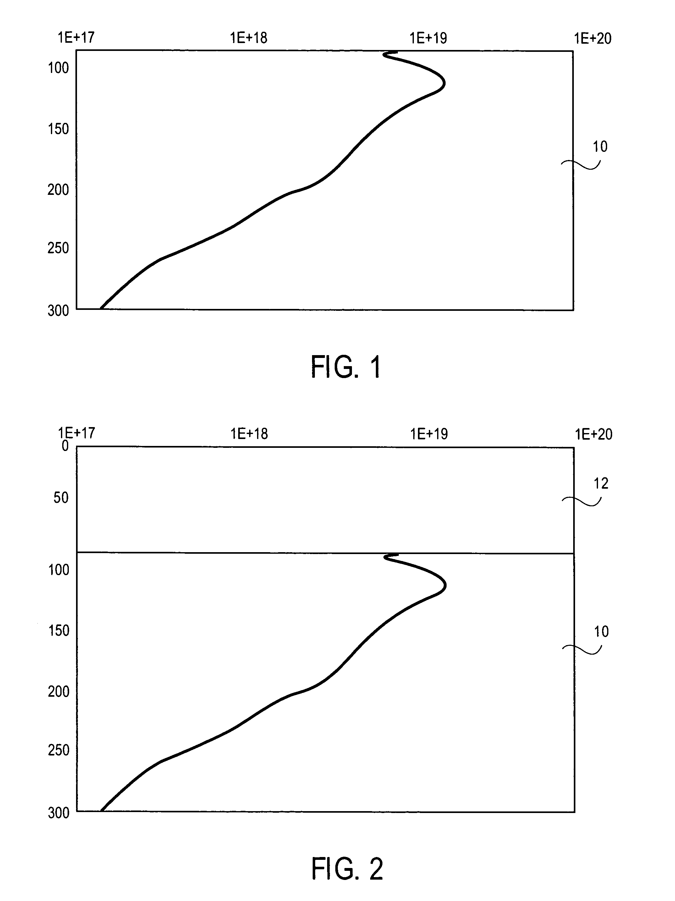
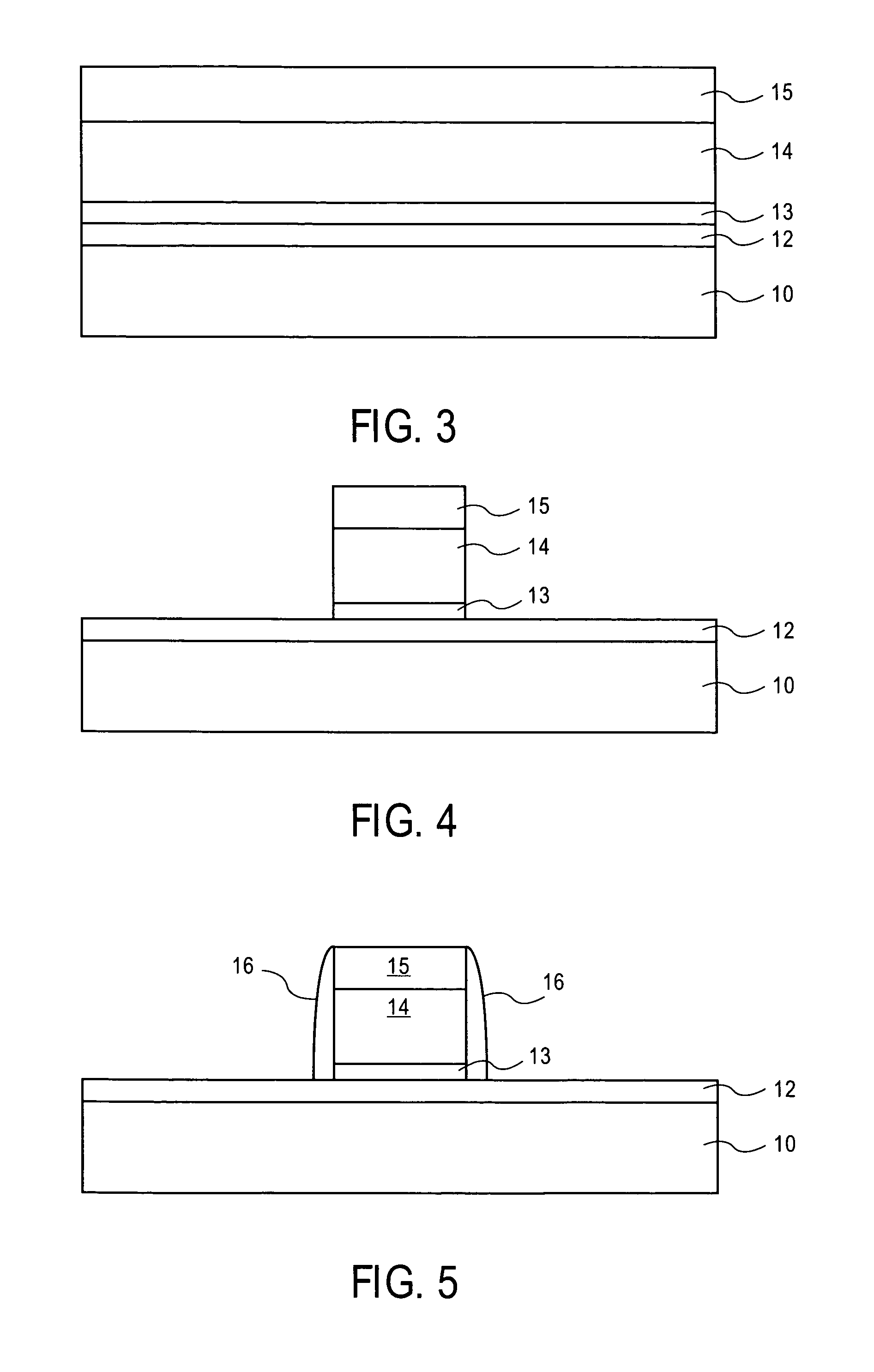
[0022]In FIG. 1, the upper approximately 200 nanometers (nm) of a monocrystalline silicon substrate 10 is illustrated. As shown, the upper region of this substrate is heavily doped with a dopant such as boron. The doping profile illustrates that the doping level has a peak below the surface in excess of 1019 atoms / cm3, or higher. This doping pro...


PUM

PropertyMeasurementUnit
work functionaaaaaaaaaa

Abstract

An MOS transistor formed on a heavily doped substrate is described. Metal gates are used in low temperature processing to prevent doping from the substrate from diffusing into the channel region of the transistor.

Description

FIELD OF THE INVENTION[0001]The invention relates to the field of MOS transistors, particularly those fabricated with epitaxial source and drain regions.PRIOR ART AND RELATED ART[0002]Delta-doped transistors are described in Noda et al. “0.1 μm Delta-Doped MOSFET Using Post Low Energy Implanting Selective Epitaxy,”VLSI Technology 1994. Digest of Technical Papers. The motivation for the Delta-doped transistor is that higher mobility (less impurity scattering) is achieved with an un-doped or lightly doped channel. Such devices are also described in patent application Ser. No. 10 / 692,696, filed Oct. 24, 2003, titled “Epitaxially Deposited Source / Drain,” assigned to the assignee of the present application.[0003]The fabrication of these transistors relies in large part upon the difference in the doping levels between the heavily doped substrate and the lightly doped or un-doped epitaxially formed surface of the substrate. An etchant is able to discriminate between the surface region and ...

Claims


Application Information

Patent Timeline
Patent Type & Authority Patents(United States)
IPC IPC(8): H01L21/302
CPCH01L21/28079H01L21/28194H01L29/41775H01L29/495H01L29/517H01L29/66545H01L29/6656H01L29/66606H01L29/66636H01L29/7834H01L29/51H01L29/518Y10S438/926Y10S438/957H01L29/66628H01L29/0673H01L29/42392H01L29/66742H01L29/78618H01L29/78696
Inventor LINDERT, NICKBRASK, JUSTIN K.WESTMEYER, ANDREW
Owner TAHOE RES LTD
Why Eureka
Try Eureka