Efficient white-light OLED display with filters

a technology of oled display and filter, which is applied in the direction of discharge tube luminescnet screen, discharge tube/lamp details, electric discharge lamps, etc., can solve the problems of reducing the efficiency of three-layer structure, difficult to achieve light emission with strong intensity, and manufacturing difficulties, so as to improve power efficiency, improve color gamut, and reduce voltage requirements

Active Publication Date: 2008-02-19
GLOBAL OLED TECH
View PDF23 Cites 17 Cited by
  • Summary
  • Abstract
  • Description
  • Claims
  • Application Information

AI Technical Summary

Benefits of technology

[0017]It is an advantage of the present invention that it provides for a device with improved color gamut and improved power efficiency, with lower voltage requirements, high stability, and better angular dependence.
that it provides for a device with improved color gamut and improved power efficiency, with lower voltage requirements, high stability, and better angular dependence.

Problems solved by technology

This produces manufacturing difficulties.
However, it is difficult to achieve light emission with strong intensity in the red, green, and blue portions of the spectrum.
It is known to use a third light-emitting layer to provide a third intensive emission peak, but such a three-layer structure shows diminished efficiency.
Although luminance efficiency is increased, this tandem white OLED device has weaker green and red color components in the spectrum.
Although color emission and luminance efficiency is improved, this tandem white OLED cannot be made with less than three EL units, implying that it requires a drive voltage at least 3 times as high as that of a conventional OLED.

Method used


Image

  • Efficient white-light OLED display with filters
  • Efficient white-light OLED display with filters
  • Efficient white-light OLED display with filters

Examples


example 1

Comparative Two-layer

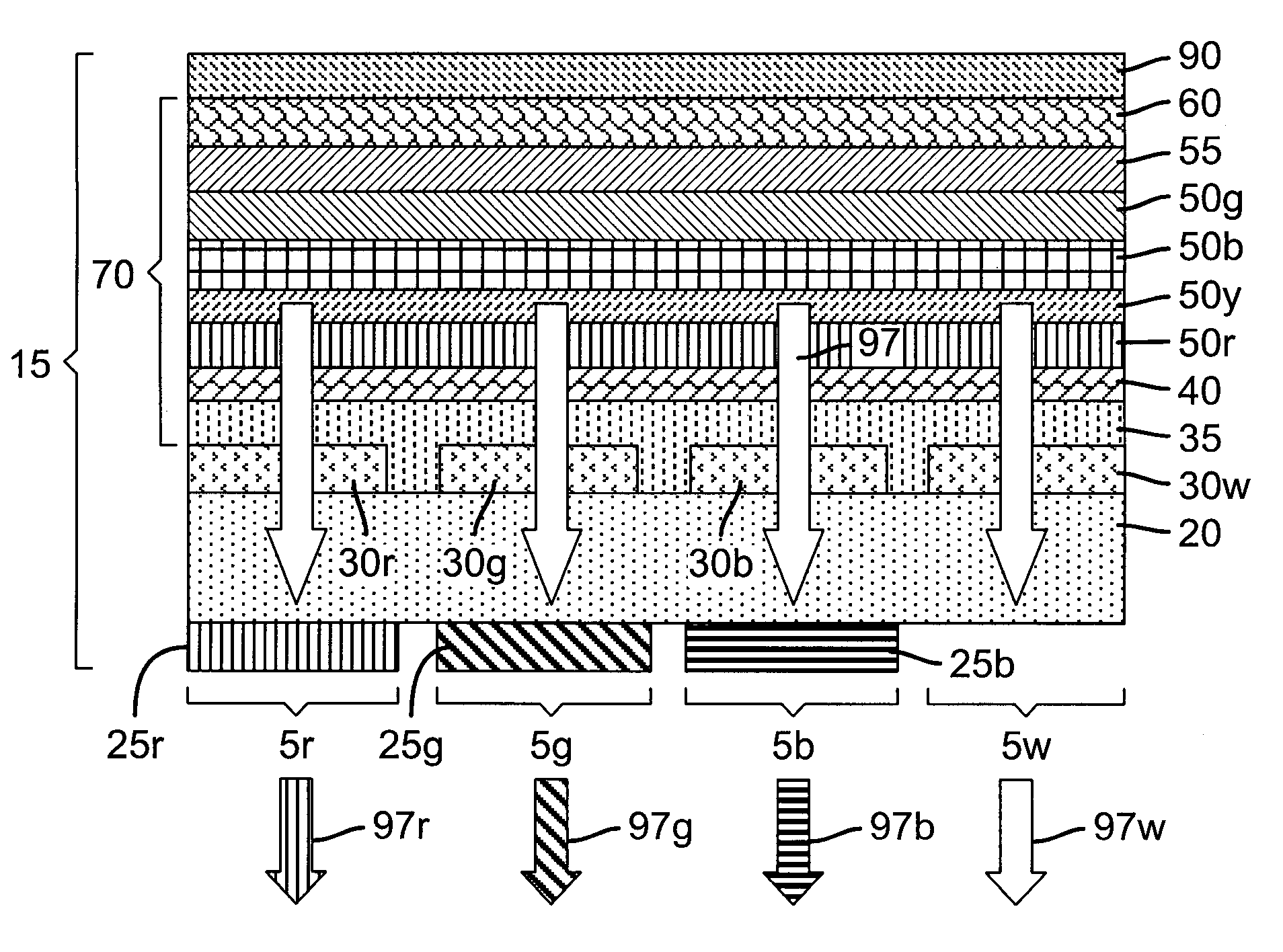
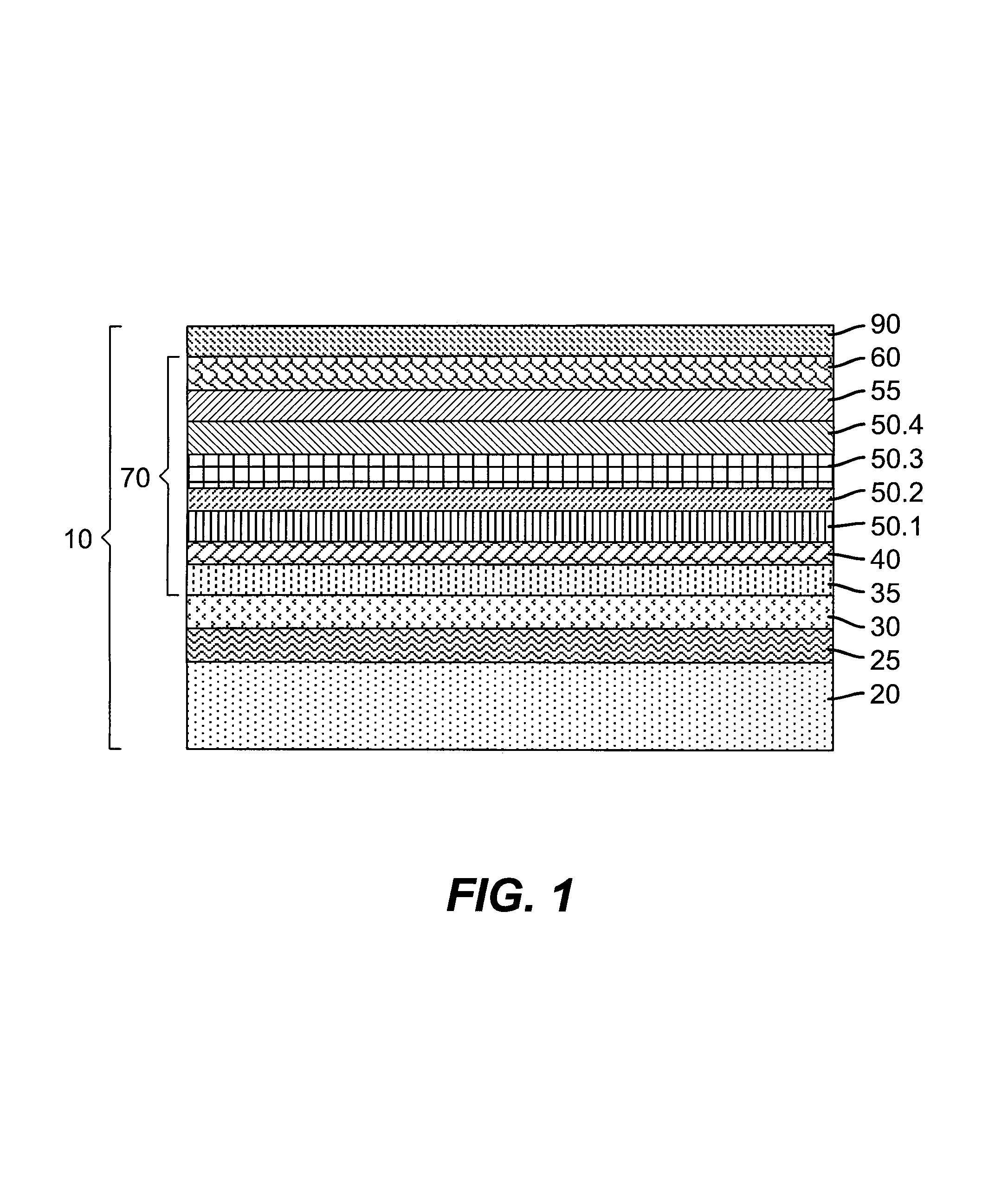
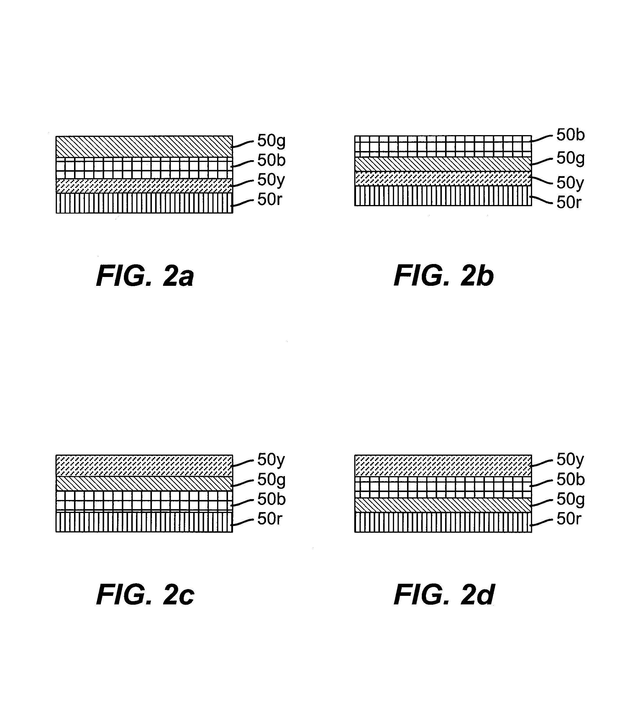
[0114]A comparative color OLED display was constructed in the following manner:[0115]1. A clean glass substrate was deposited by sputtering with indium tin oxide (ITO) to form a transparent electrode of 85 nm thickness.[0116]2. The above-prepared ITO surface was treated with a plasma oxygen etch.[0117]3. The above-prepared substrate was further treated by vacuum-depositing a 10 nm layer of hexacyanohexaazatriphenylene (CHATP) as a hole-injecting layer (HIL).

[0118][0119]4. The above-prepared substrate was further treated by vacuum-depositing a 10 nm layer of 4,4′-bis[N-(1-naphthyl)-N-phenylamino]biphenyl (NPB) as a hole-transporting layer (HTL).[0120]5. The above-prepared substrate was further treated by vacuum-depositing a 20 nm yellow light-emitting layer including 14 nm NPB (as host) and 6 nm 9,10-bis(2-naphthyl)anthracene (ADN) as a stabilizer with 2% yellow-orange emitting dopant diphenyltetra-t-butylrubrene (PTBR).

[0121][0122]6. The above-prepared substrate...

example 2

Comparative Three-layer

[0126]A comparative color OLED display was constructed in the following manner:[0127]1. A clean glass substrate was deposited by sputtering with ITO to form a transparent electrode of 60 nm thickness.[0128]2. The above-prepared ITO surface was treated with a plasma oxygen etch.[0129]3. The above-prepared substrate was further treated by vacuum-depositing a 10 nm layer of CHATP as a hole-injecting layer (HIL).[0130]4. The above-prepared substrate was further treated by vacuum-depositing a 10 nm layer of NPB as a hole-transporting layer (HTL).[0131]5. The above-prepared substrate was further treated by vacuum-depositing a 20 nm red light-emitting layer including 14 nm of NPB and 6 nm BNA as a stabilizer doped with 0.5% dibenzo {[f,f′]-4,4′7,7′-tetraphenyl]diindeno-[1,2,3-cd:1′,2′,3′-lm]perylene (TPDBP) as a red emitting dopant.[0132]6. The above-prepared substrate was further treated by vacuum-depositing a 15 nm blue light-emitting layer including 14 nm BNA host...

example 3

Inventive

[0136]An inventive color OLED display was constructed in the following manner:[0137]1. A clean glass substrate was deposited by sputtering with ITO to form a transparent electrode of 60 nm thickness.[0138]2. The above-prepared ITO surface was treated with a plasma oxygen etch.[0139]3. The above-prepared substrate was further treated by vacuum-depositing a 10 nm layer of CHATP as a hole-injecting layer (HIL).[0140]4. The above-prepared substrate was further treated by vacuum-depositing a 10 nm layer of NPB as a hole-transporting layer (HTL).[0141]5. The above-prepared substrate was further treated by vacuum-depositing a 18 nm red light-emitting layer including 12.6 nm of NPB and 5.4 nm BNA as a stabilizer doped with 0.5% TPDBP as a red emitting dopant.[0142]6. The above-prepared substrate was further treated by vacuum-depositing a 2 nm yellow light-emitting layer including 1.4 nm NPB (as host) and 0.6 nm ADN as a stabilizer with 3% yellow-orange emitting dopant PTBR.[0143]7....


PUM


Abstract

A white light-emitting OLED device comprising: an anode and a cathode; at least four light-emitting layers provided between the anode and the cathode, wherein each of the four light-emitting layers produces a different emission spectrum when current passes between the anode and cathode, and such spectra combine to form white light; and wherein the four light-emitting layers include a red light-emitting layer, a yellow light-emitting layer, a blue light-emitting layer, and a green light-emitting layer, arranged such that: i) each of the light-emitting layers is in contact with at least one other light-emitting layer, ii) the blue light-emitting layer is in contact with the green light-emitting layer, and iii) the red light-emitting layer is in contact with only one other light-emitting layer.

Description

CROSS REFERENCE TO RELATED APPLICATIONS[0001]Reference is made to commonly assigned U.S. Patent Publication No. 2005 / 0181232, published Aug. 18, 2005, entitled “Anthracene Derivative Host Having Ranges Of Dopants” by Ricks et al.; U.S. Patent Publication No. 2005 / 0181232, published Nov. 10, 2005, entitled “Improved Tuned Microcavity Color OLED Display” by Hatwar et al.; and U.S. patent application Ser. No. 11 / 170,681, filed Jun. 29, 2006, entitled “White Light Tandem Oled Display With Filters” by Hatwar et al.; the disclosures of which are incorporated herein by reference.FIELD OF THE INVENTION[0002]The present invention relates to broadband light-producing OLED displays with color filters.BACKGROUND OF THE INVENTION[0003]An organic light-emitting diode device, also called an OLED, commonly includes an anode, a cathode, and an organic electroluminescent (EL) unit sandwiched between the anode and the cathode. The organic EL unit includes at least a hole-transporting layer (HTL), a li...

Claims


Application Information

Patent Timeline
Patent Type & Authority Patents(United States)
IPC IPC(8): H01J1/62H01J63/04
CPCH01L27/3213H01L51/5278H01L51/5036H01L27/3244H01L51/0053H01L51/0054H01L51/0072H01L51/0073H01L51/008H01L51/0071H10K59/351H10K59/12H10K85/621H10K85/622H10K85/322H10K85/6574H10K85/657H10K85/6572H10K50/125H10K50/19H10K2102/351
Inventor HATWAR, TUKARAM K.SPINDLER, JEFFREY P.
Owner GLOBAL OLED TECH
Why Eureka
Try Eureka