Semiconductor circuit, display device, electronic apparatus
a technology of semiconductors and circuits, applied in logic circuit coupling/interface arrangements, pulse techniques, instruments, etc., can solve the problems of reduced yield, increased layout area, and reduced yield, so as to reduce layout area, reduce variation in performance, and improve yield
- Summary
- Abstract
- Description
- Claims
- Application Information
AI Technical Summary
Benefits of technology
Problems solved by technology
Method used
Image
Examples
embodiment mode 1
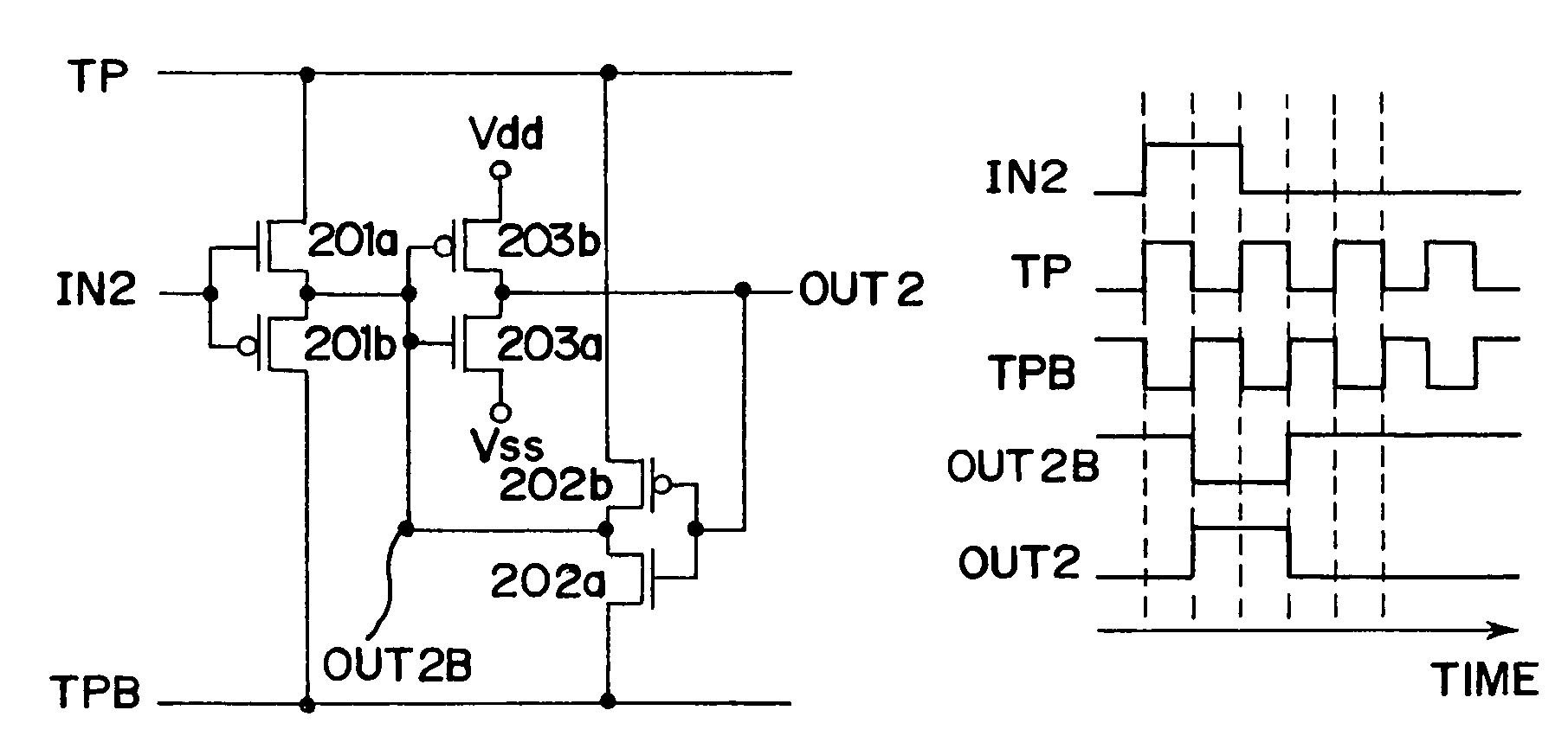
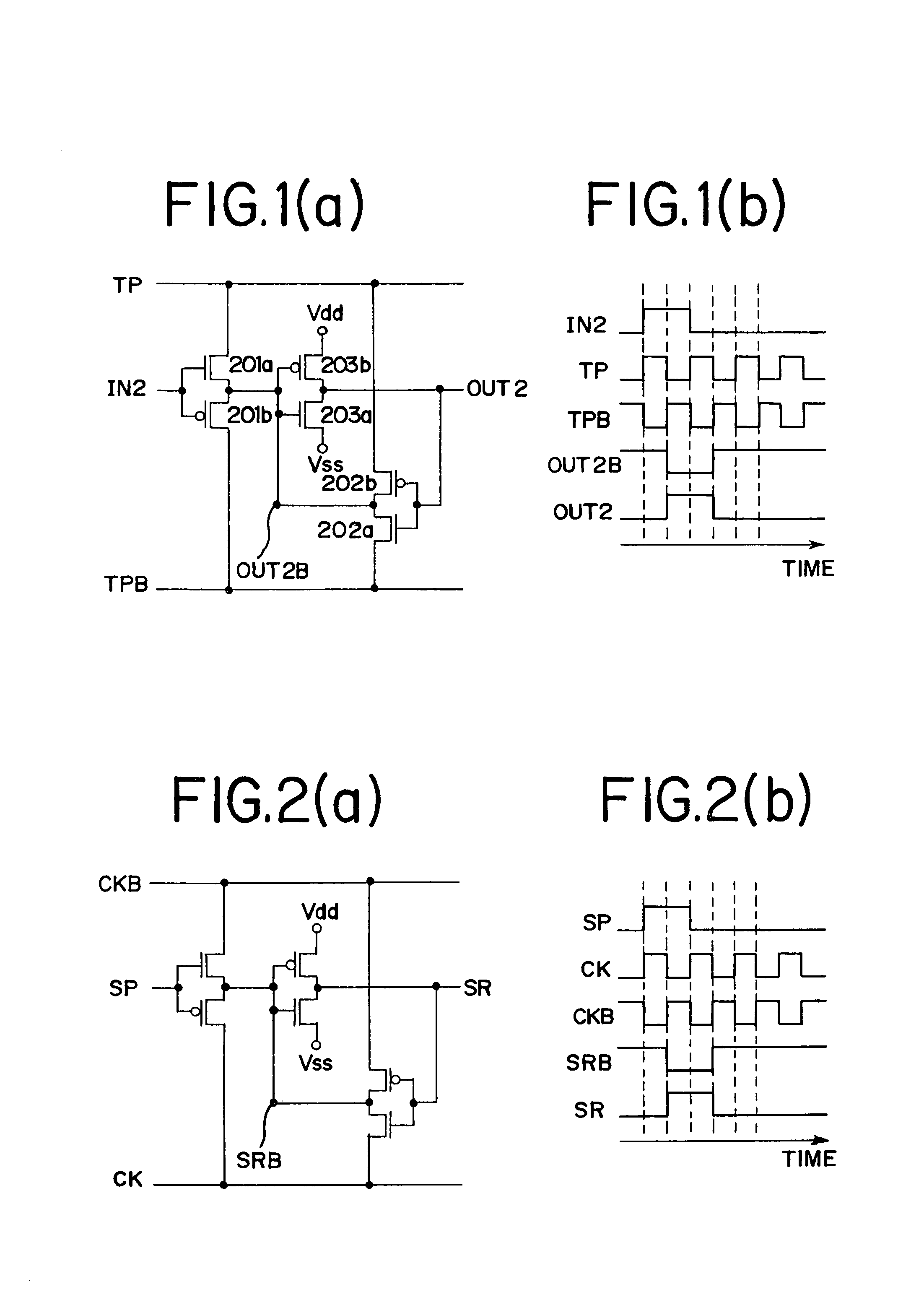
[0065]FIG. 1(a) shows one embodiment mode of a semiconductor circuit of the invention. As shown in FIG. 1(a), the first clocked inverter CKINV1 and the second clocked inverter CKINV2 of a conventional semiconductor circuit are replaced by circuits constructed of n-channel transistors and p-channel transistors. Here, the n-channel transistors and the p-channel transistors correspond to a first n-channel transistor 201a, a first p-channel transistor 201b, a second n-channel transistor 202a, and a second p-channel transistor 202b. In this specification, a terminal to serve as a source electrode or a drain electrode of the first n-channel transistor 201a, and a terminal to serve as a source electrode or a drain electrode of the second p-channel transistor 202b, to each of which a timing control signal TP is inputted, are called first terminals. In addition, a terminal to serve as a source electrode or a drain electrode of the first p-channel transistor 201b, and a terminal to serve as a...
embodiment 1
[0083]Description is made below on an embodiment of the invention.
[0084]FIG. 2(a) is a circuit constructed for the purpose of using the semiconductor circuit of the invention as a shift register circuit. Here, a start pulse SP is used as the input signal IN, a clock signal CK is used as the timing control signal TP, and an inverted clock signal CKB is used as the inverted timing control signal TPB. In addition, the circuit outputs SR.
[0085]FIG. 2(b) shows a timing chart of FIG. 2(a). Description on the operation of the timing chart in FIG. 2(b) is omitted since it is shown in Embodiment Mode 1.
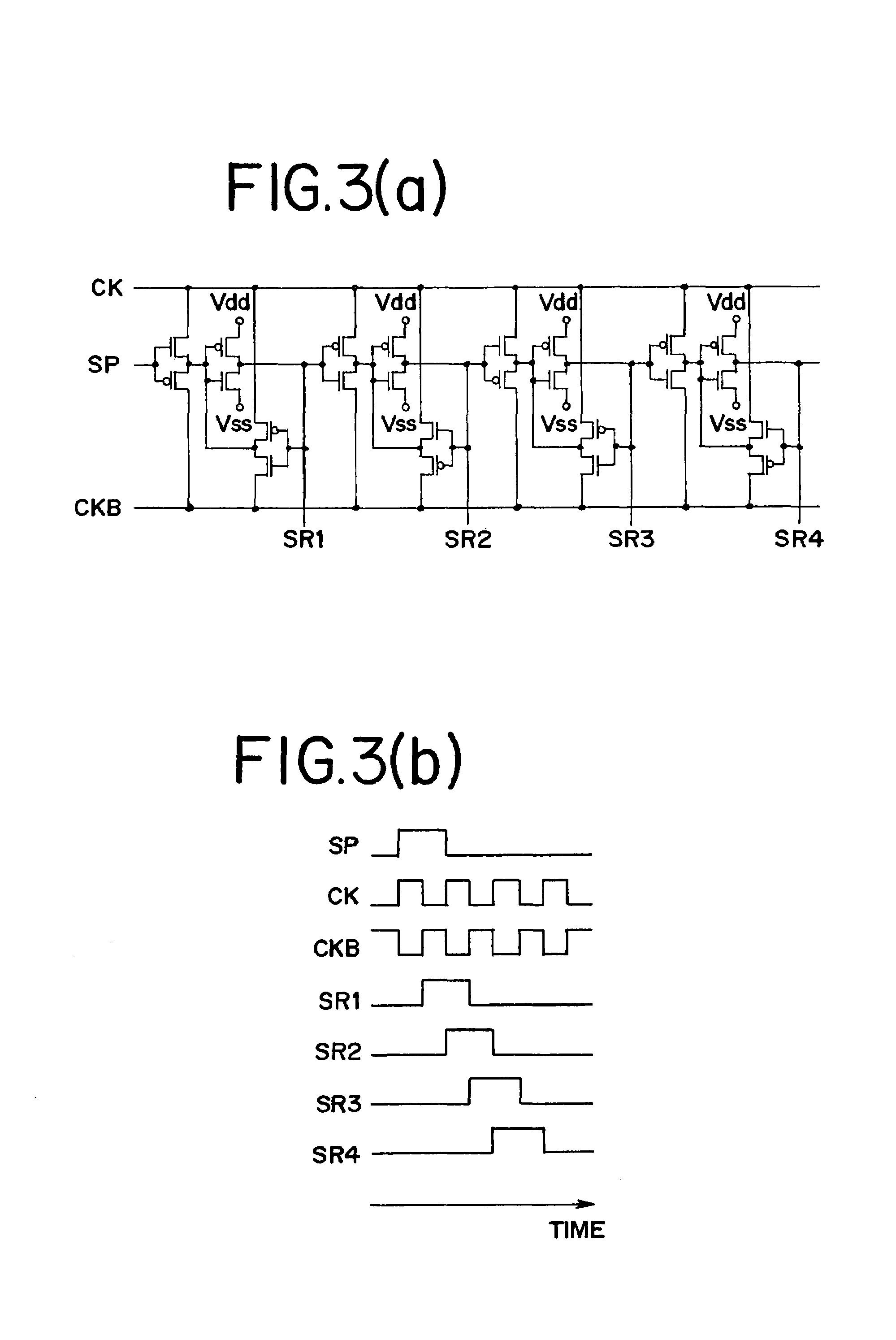
[0086]FIG. 3(a) shows an example where four stages of the shift register circuit in FIG. 2(a) are used. FIG. 3(b) shows a timing chart thereof. Note that an output of a first-stage shift register is SR1, an output of a second-stage shift register is SR2, an output of a third-stage shift register is SR3, and an output of a fourth-stage shift register is SR4.
[0087]In constructing multiple stages...
embodiment 2
[0091]FIG. 5(a) is a circuit constructed for the purpose of using the semiconductor circuit of the invention as a latch circuit. Here, a data signal DATA is used as the input signal IN, a sampling pulse LSP is used as the timing control signal TP, and an inverted sampling pulse LSPB is used as the inverted timing control signal TPB. In addition, the circuit outputs D_OUT.
[0092]FIGS. 5(b), (c), (d) and (e) show timing charts of FIG. 5(a). Note that an initial state of the output D_OUT is at “Lo”. As for the operation of the timing charts in FIGS. 5(b), (c), (d) and (e), the data signal DATA is sampled when the sampling pulse LSP is at “Lo” whereas the previous output is held when the sampling pulse LSP is at “Hi” as shown in Embodiment Mode 1. In each of the timing charts, it can be seen that the data signal DATA right before the sampling pulse LSP changes from “Lo” to “Hi” continues to be held.
[0093]FIG. 6(a) is a diagram showing an example of actually designing the latch circuit. F...
PUM
 Abstract
Description
Claims
Application Information


