Shift register

a technology of shift register and drive circuit, which is applied in the direction of digital storage, counting chain synchronous pulse counters, instruments, etc., can solve the problems of constant deterioration increased voltage of thin film transistors, and worse mobility

Active Publication Date: 2008-02-19
LG DISPLAY CO LTD
View PDF8 Cites 54 Cited by
  • Summary
  • Abstract
  • Description
  • Claims
  • Application Information

AI Technical Summary

Benefits of technology

[0030]Other systems, methods, features and advantages of the invention will be, or will become, apparent to one with skill in the art upon examination of the following figures and detailed description. It is intended that all such additional systems, methods, features and advantages be included within this description, be within the scope of the invention, and be protected by the following claims.

Problems solved by technology

However, if a high voltage is continuously applied to the gate terminal of the thin film transistor, i.e., the second output terminal Qb, the threshold voltage of the thin film transistor increases to make the mobility grow worse.
In this way, if the threshold voltage increases due to long time use, the thin film transistor is continuously deteriorated.
In other words, if the voltage is continuously applied to the second output terminal Qb, there is a problem in that damage of the device or malfunction by the deterioration of the thin film transistor is generated.

Method used


Image

  • Shift register
  • Shift register
  • Shift register

Examples


first embodiment

[0068]FIG. 7 Is a diagram representing a drive waveform for driving a shift register of FIGS. 5 and 6 and an output waveform in accordance therewith. A driving method of the shift register according to the present invention will be explained with reference to FIG. 7 in conjunction with reference to FIGsS 5 and 6.

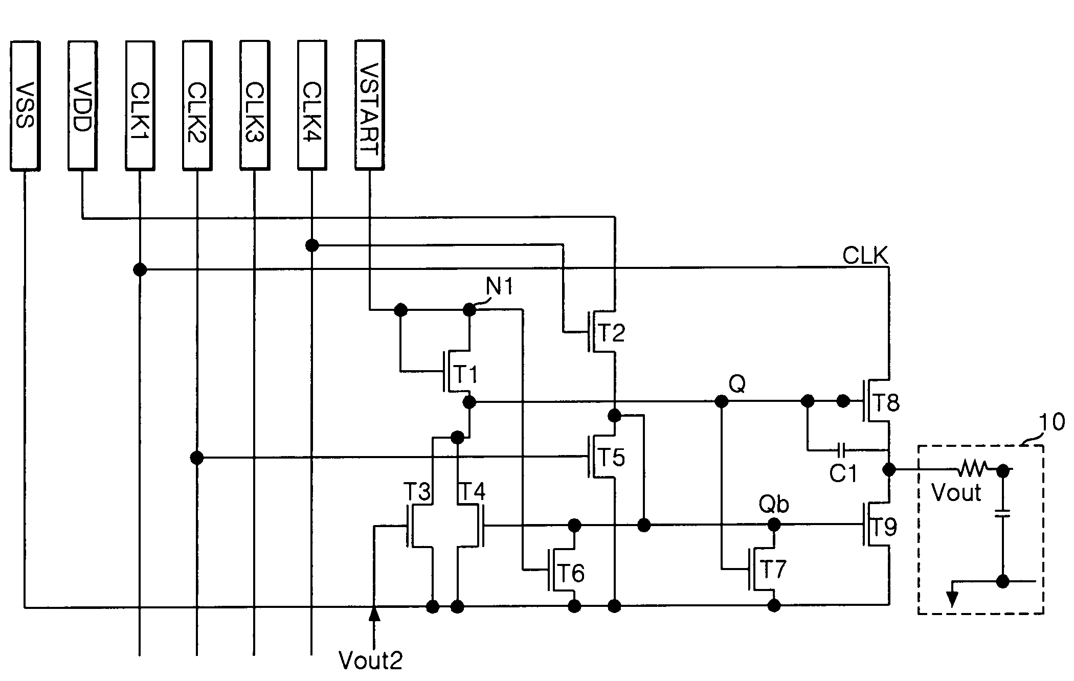
[0069]In a T1 period, the start pulse or the previous stage's output signal is inputted in synchronization with the fourth clock signal CLK4. If the start pulse Vstart is inputted, the first NMOS transistor T1 is turned on and the Q node is charged with as much voltage as the start pulse Vstart. At the same time, if the fourth clock signal CLK4 is inputted, the second NMOS transistor T2 is turned on and the Qb node is charged with the voltage from the second voltage supply source VDD. However, the sixth NMOS transistor T6 is turned on by the start pulse Vstart and the seventh NMOS transistor T7 is turned on by the voltage charged in the Q node, thus the voltage charged in th...

second embodiment

[0125]Hereinafter, the operation of the shift register of the T2 period to the T8 period is the same as the foregoing second embodiment, thus the detail explanation on this will be omitted.

[0126]It is desirable that the penod during which the logic value of the Qb node is high, and while the logic value of the output signal line is low, includes a clock signal when the output signal of the pertinent stage is generated, e.g., the period when the first clock signal is inputted in the first stage.

[0127]The present invention can reduce the accumulated voltage stress which is generated by a continuous voltage application to the Qb node. Further, the shift register and driving method thereof can be driven by a two-phase, a three-phase or a five-phase clock.

[0128]FIG. 11 is a diagram briefly representing the configuration of the shift register of the present invention, and represents an example of using a two phase clock in a simple circuit.

[0129]Referring to FIG. 11, the shift register in...


PUM


Abstract

A shift register has a plurality of stages which output driving signals, each stage including a pull-up transistor to output a first clock signal in response to a logic value of a Q node; a pull-down transistor to supply a voltage from a first voltage supply source to the output in response to a logic value of a Qb node; a Q node controller to control the logic value of the Q node in response to any one of the previous stage's output signal and the next stage's output signal; and a Qb node controller to control the logic value of the Qb node to alternate repeatedly between low and high by use of at least one of a second clock signal, a third clock signal and the logic value of the Q node when the output signal is in a low state.

Description

PRIORITY CLAIM[0001]This application claims the benefit of the Korean Patent Application No. P2004-118605 filed on Dec. 31, 2004, which is hereby incorporated by reference.BACKGROUND OF THE INVENTION[0002]1. Field of the Invention[0003]The present invention relates to a drive circuit of a display device, and more particularly to a shift register that is adaptive for preventing malfunction and damage, and a driving method thereof.[0004]2. Description of the Related Art[0005]Recently, there have been developed various flat panel display devices that can reduce their weight and size which is an advantage over a cathode ray tube CRT. The flat panel display device includes a liquid crystal display LCD, a field effect display FED, a plasma display panel PDP, an electro luminescence EL display device and so on.[0006]The liquid crystal display (hereinafter, referred to as “LCD”) device among the flat panel display devices has its application range on a broadening trend owing to its characte...

Claims


Application Information

Patent Timeline
Patent Type & Authority Patents(United States)
IPC IPC(8): G11C19/00
CPCG09G3/3677G11C19/00G11C19/28G09G2330/04G09G3/36H03K23/44
Inventor JANG, YONG HO
Owner LG DISPLAY CO LTD
Why Eureka
Try Eureka