Microfluidics chips and methods of using same

a technology of microfluidics and chips, applied in the field of microfluidics, can solve the problems of inability to prevent contamination of actual fluidic circuit components, difficulty and time consumption, and undesirable blood contact with the patterned surface of the wafer, and achieve the effect of reducing or overcoming

Inactive Publication Date: 2008-02-26
AGENCY FOR SCI TECH & RES +1
View PDF10 Cites 2 Cited by
  • Summary
  • Abstract
  • Description
  • Claims
  • Application Information

AI Technical Summary

Benefits of technology

[0011]The microfluidics chips and methods of the present invention reduce or overcome many deficiencies of the prior art, and in particular allow components having patterned surfaces to be reused. As used herein “reused” and “reusable” mean that the components having patterned surfaces do not have to be cleaned prior to use with another sample.

Problems solved by technology

One problem with this arrangement is that in order to reuse this wafer bonded microfluidics chip device to analyze a new sample, the microfluidics channels must be thoroughly cleaned, which is difficult and time consuming.
In most respects it is undesirable that the blood, or any related biological product, contact the patterned surfaces of the wafers.
While the patent does describe prevention of cross contamination between liquids in the card by using plastic valve membranes, there is no provision for preventing contamination of the actual fluidic circuit components.
However, the microfluidics delivery systems of this particular patent require electromechanical valves to stop and start flows of fluids, with components that are irregularly shaped, and do not employ a vacuum for shaping of barrier films.

Method used


Image

  • Microfluidics chips and methods of using same
  • Microfluidics chips and methods of using same
  • Microfluidics chips and methods of using same

Examples


Embodiment Construction

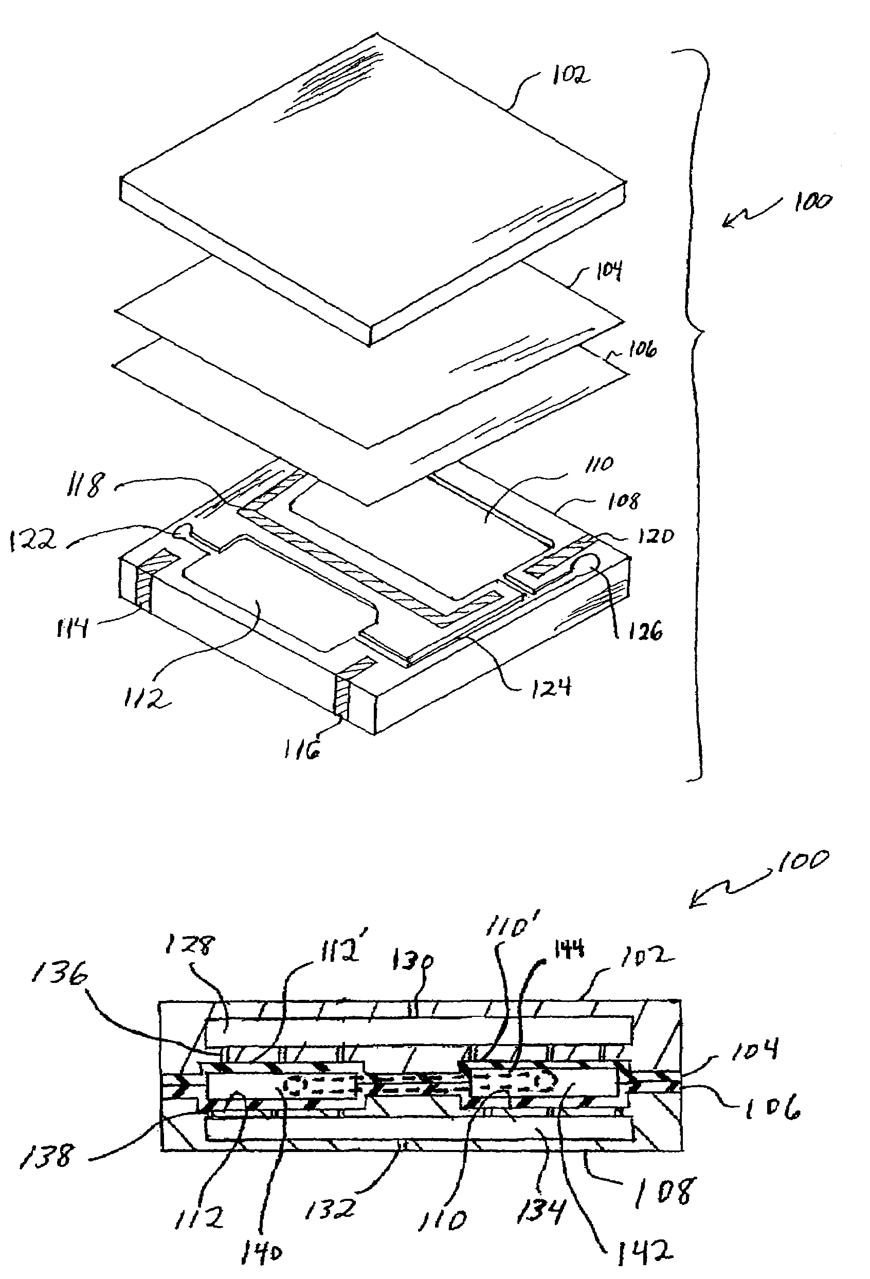
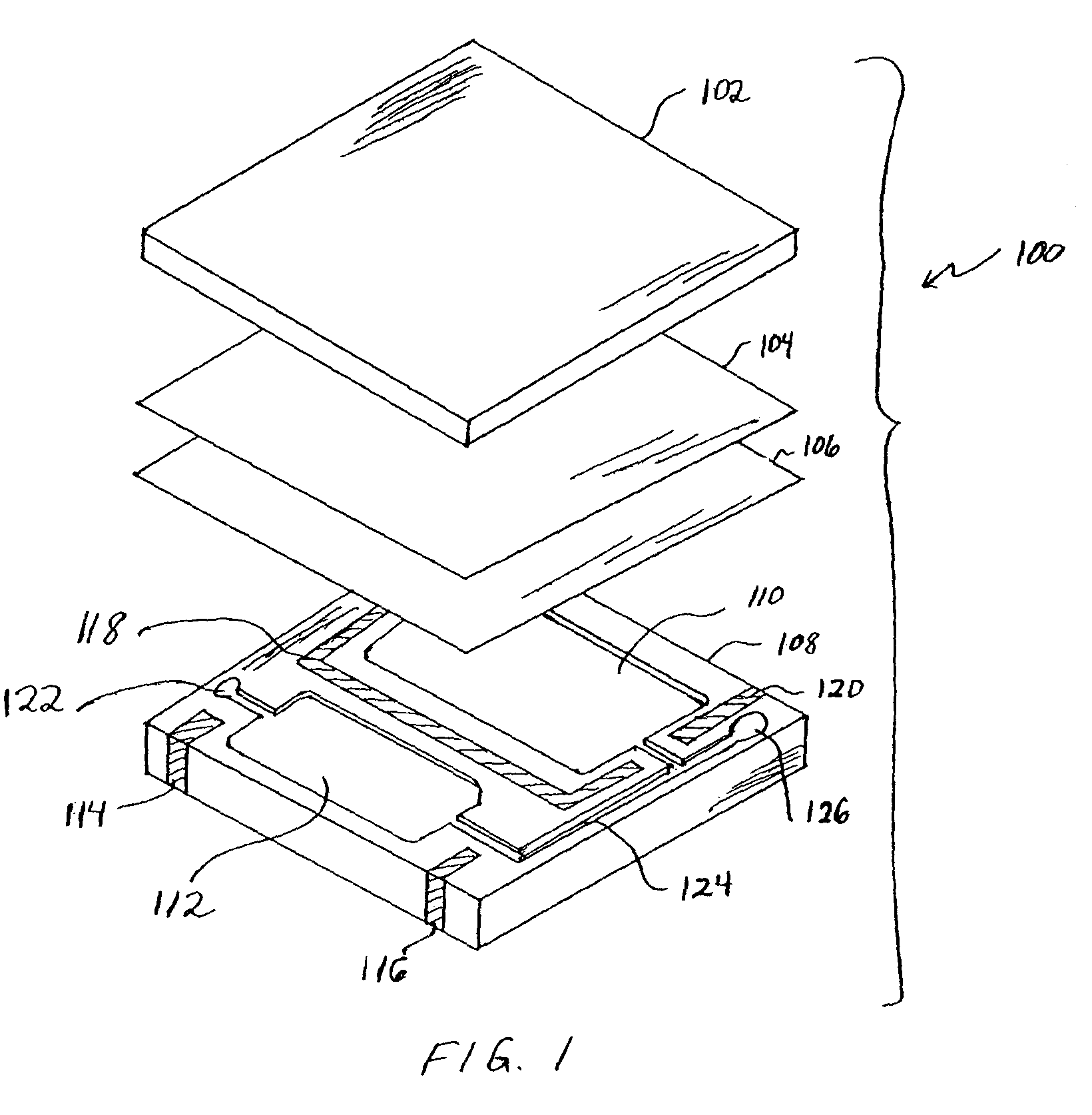
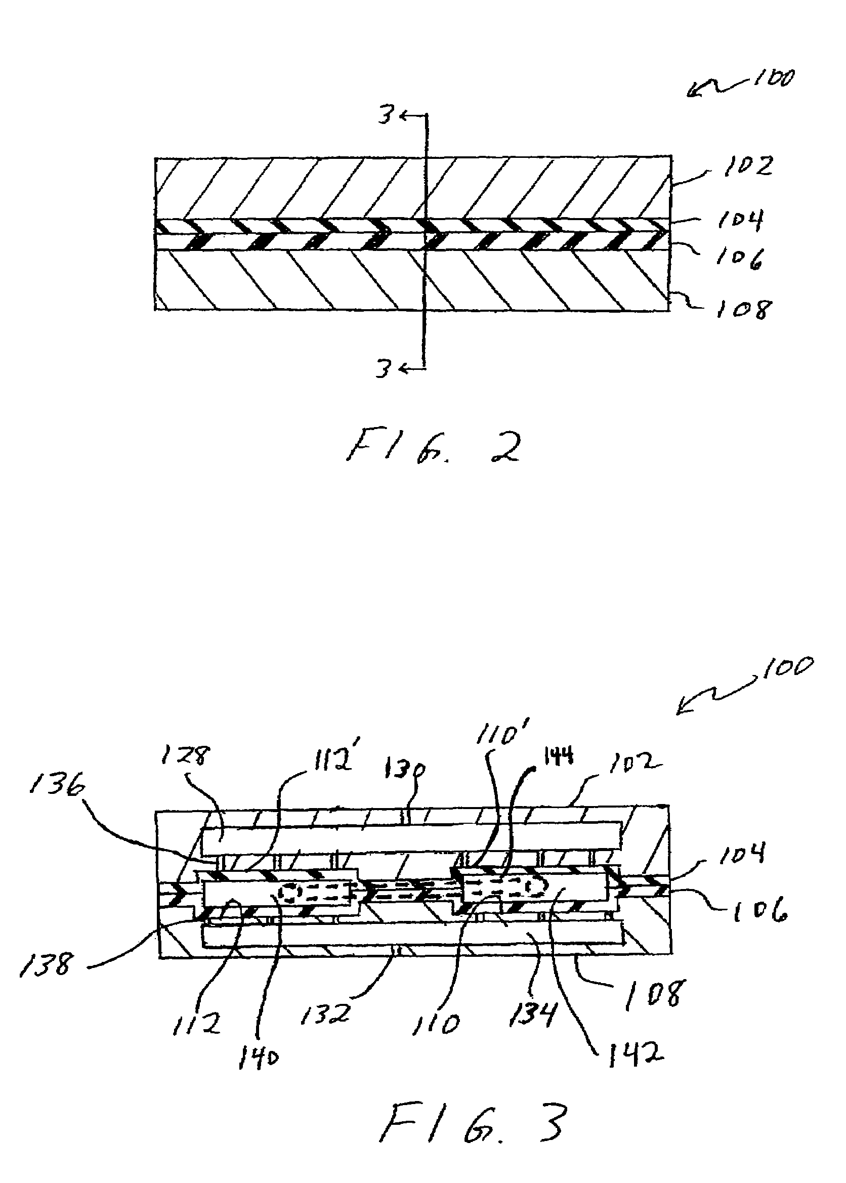
[0037]The microfluidics chips and methods of the present invention utilize thin polymeric barrier films over patterned parts. As used herein the term “patterned” includes, but is not limited to, machined parts and parts having patterns created by other methods, for example printing, embossing etching, and the like. The polymer polymeric barrier films are disposable, allowing the patterned parts to be reusable. In place of conventional wafer to wafer bonding to form microfluidics channels and chambers, the top and bottom wafers may be mechanically clamped together during operation of the chip. Between the two wafers, two thin polymer barrier films are inserted. Vacuum may be used to draw the polymeric barrier films against the patterned wafers. The two wafers are mechanically clamped together to form an assembly and is ready to use. After use of the lined microfluidics chip, the polymeric barrier films can be disposed of and the patterned parts can be reused. Since the two wafers are...


PUM

PropertyMeasurementUnit
thicknessaaaaaaaaaa
widthaaaaaaaaaa
depthaaaaaaaaaa

Abstract

Microfluidics chips and methods of use are described, comprising a pair of wafers, at least one having a patterned surface, and two polymeric barrier films between the wafers conforming to the patterned surface. The polymeric barrier films allow the wafers of the inventive microfluidics chips to be reused without cleaning.

Description

CROSS-REFERENCE TO RELATED APPLICATIONS [0001]This application is related to patent application Ser. No. 10 / 631,478, filed Jul. 31, 2003.BACKGROUND INFORMATION [0002]1. Technical Field[0003]The invention is generally related to the field of micofluidics. More specifically, the invention relates to novel microfluidics chips and methods of using same which address the problem of contamination of patterned surfaces in such devices.[0004]2. Background Art[0005]Currently known microfluidics chips typically comprise two mating halves or wafers, each having patterned surfaces. The patterns are such that when the two wafers are placed adjacent each other, a microfluidics cavity or flow channel is formed between the wafers. The two wafers are bound together in a process referred to as wafer bonding. One or more fluids is forced through the microfluidics channel, for example a sample and a reagent. One problem with this arrangement is that in order to reuse this wafer bonded microfluidics chi...

Claims


Application Information

Patent Timeline
Patent Type & Authority Patents(United States)
IPC IPC(8): H01L23/34B01L3/00B81C3/00
CPCB01L3/502707B81C3/001B01L2200/0689B01L2200/12B01L2200/141Y10T156/10B01L2300/1827B81B2201/058B01L2300/0887Y10T137/2196
Inventor SAMPER, VICTORCONG, LINJI, HONGMIAO
Owner AGENCY FOR SCI TECH & RES
Why Eureka
Try Eureka