MOSFET devices and methods for making them

a technology of metal oxides and transistors, applied in the direction of semiconductor devices, basic electric elements, electrical apparatus, etc., can solve the problems of higher gate leakage, fermi level pinning, and problem, and achieve the effect of not affecting the performance of the structur

Active Publication Date: 2010-10-12
INTERUNIVERSITAIR MICRO ELECTRONICS CENT (IMEC VZW) +1
View PDF6 Cites 0 Cited by
  • Summary
  • Abstract
  • Description
  • Claims
  • Application Information

AI Technical Summary

Benefits of technology

[0007]The present invention, in one aspect, relates to a MOSFET structure with a high-k material as gate dielectric and a gate electrode such as a polysilicon gate electrode. An advantage of embodiments of the present invention is that the performance of the structure is not affected adversely.
[0008]The present invention, in another aspect, relates to the provision of a method to manufacture such a MOSFET structure. An advantage of some embodiments of the present invention is that the method can reduce or overcome at least one drawback of prior art methods, and that a MOSFET structure can be provided with improved performance compared to prior art devices.

Problems solved by technology

Scaling MOSFET transistors to improve performance results in higher gate leakage as the SiO2 gate dielectric becomes thinner.
With the introduction of the high-k dielectrics a new problem appeared: Fermi level pinning.
The Fermi level pinning effect occurs at the polysilicon (poly-Si) / metal oxide interface and causes high threshold voltages in MOSFET devices.
However, it has been proven difficult to identify band-edge metals (metals with either a n-type or a p-type work function (WF)) that are compatible with the conventional CMOS (Complementary Metal-Oxide-Semiconductor) manufacturing process.
In either case, a selective removal of one of the metal gates and / or dielectrics is necessary and adds substantial complexity and costs to the manufacturing process.
On small devices, the phase or composition of the FUSI gates tends to distribute unevenly, which can result in severe within-wafer threshold voltage (Vt) non-uniformity.

Method used


Image

  • MOSFET devices and methods for making them
  • MOSFET devices and methods for making them
  • MOSFET devices and methods for making them

Examples


first embodiment

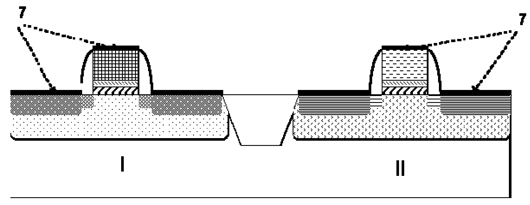
[0056]In the first aspect of the present invention, the semiconductor device comprises a MOSFET transistor, which can be either a NMOS or a PMOS transistor.

second embodiment

[0057]In the first aspect of the present invention, the semiconductor device comprises at least two MOSFET transistors, either NMOS or PMOS, with different doping levels.

third embodiment

[0058]In the first aspect of the present invention, the semiconductor device comprises at least two MOSFET transistors with opposite conductivity types, e.g. a NMOS and a PMOS transistor.

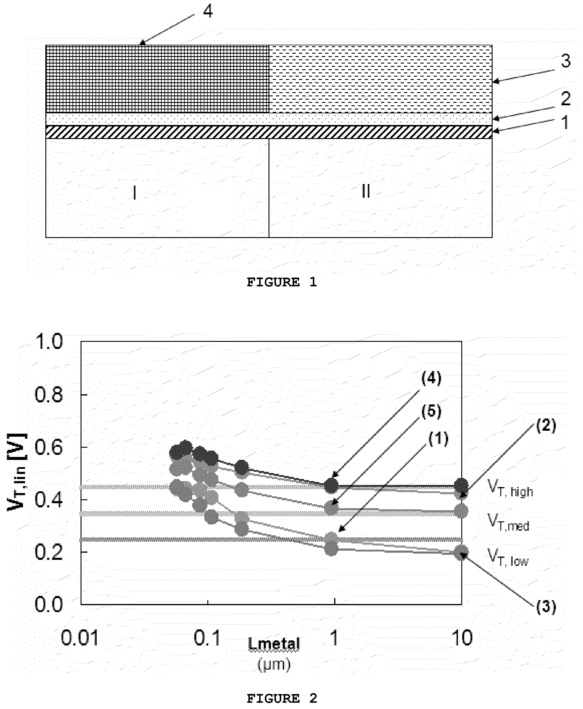
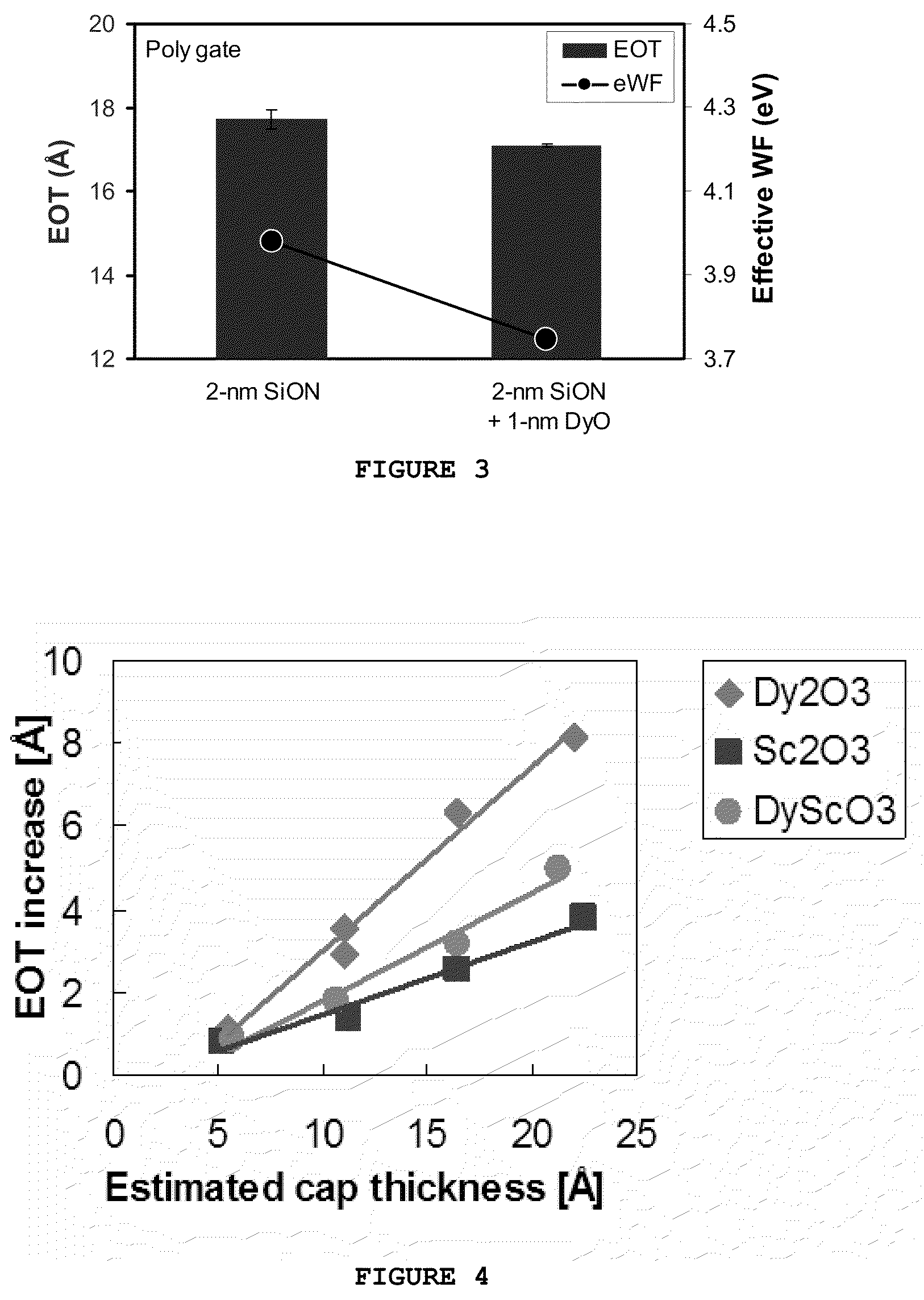
[0059]In one embodiment of the first aspect of the present invention the dielectric capping layer has a thickness smaller than 2 nm, preferably smaller than 1.5 nm and even more preferably smaller than 1 nm and comprises Scandium (Sc) based materials, e.g. Sc oxides, Sc-silicates, or combinations thereof.

[0060]The high-k dielectric layer (1) can be, for example, selected from the group consisting of SiON, HfSiOx, HfO2, ZrO2 and mixtures thereof. These can present the advantage of a stable, high quality dielectric barrier between the gate electrode, and the channel region of the semiconductor structures forming the semiconductor device.

[0061]The substrate can, for example, comprise Si, Silicon-On-Insulator (SOI), Ge, Germanium on Insulator (GeOI), III-V materials or combinations thereof. The III-V ma...


PUM


Abstract

A semiconductor device is disclosed. The device comprises a first MOSFET transistor. The transistor comprises a substrate, a first high-k dielectric layer upon the substrate, a first dielectric capping layer upon the first high-k dielectric, and a first gate electrode made of a semiconductor material of a first doping level and a first conductivity type upon the first dielectric capping layer. The first dielectric capping layer comprises Scandium.

Description

CROSS-REFERENCE TO RELATED APPLICATIONS[0001]This application claims priority under 35 U.S.C. §119 to U.S. Provisional Patent Application Ser. No. 60 / 974,039, filed Sep. 20, 2007; and to European Patent Application no. 08156018.7, filed May 9, 2008, each of which is hereby incorporated herein by reference in its entirety.FIELD OF THE INVENTION[0002]The present invention relates generally to semiconductor devices comprising a MOSFET (Metal-Oxide-Semiconductor Field Effect Transistor), and methods for making them. The present invention relates more particularly to MOSFET transistors having a gate stack comprising a material with high dielectric constant and doped poly-silicon as gate electrode, and methods for making them.TECHNICAL BACKGROUND[0003]Scaling MOSFET transistors to improve performance results in higher gate leakage as the SiO2 gate dielectric becomes thinner. To address this issue, SiO2 gate dielectric are often replaced with high-k dielectrics. A high-k dielectric is a di...

Claims


Application Information

Patent Timeline
Patent Type & Authority Patents(United States)
IPC IPC(8): H01L29/78H01L21/8238H01L21/336H01L21/3205H01L21/4763H01L29/49H01L29/51
CPCH01L21/28035H01L21/28194H01L21/823857H01L29/4916H01L29/513H01L29/517
Inventor CHANG, SHIH-HSUNRAGNARSSON, LARS-AKE
Owner INTERUNIVERSITAIR MICRO ELECTRONICS CENT (IMEC VZW)
Why Eureka
Try Eureka