

Mosfet devices and methods for making them
- Summary
- Abstract
- Description
- Claims
- Application Information
AI Technical Summary
Benefits of technology
Problems solved by technology
Method used
Image

Examples
first embodiment
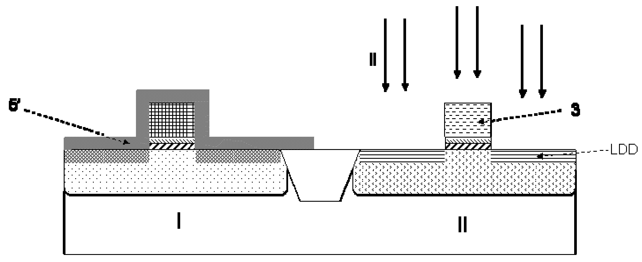
[0056]In the first aspect of the present invention, the semiconductor device comprises a MOSFET transistor, which can be either a NMOS or a PMOS transistor.
second embodiment
[0057]In the first aspect of the present invention, the semiconductor device comprises at least two MOSFET transistors, either NMOS or PMOS, with different doping levels.
third embodiment
[0058]In the first aspect of the present invention, the semiconductor device comprises at least two MOSFET transistors with opposite conductivity types, e.g. a NMOS and a PMOS transistor.
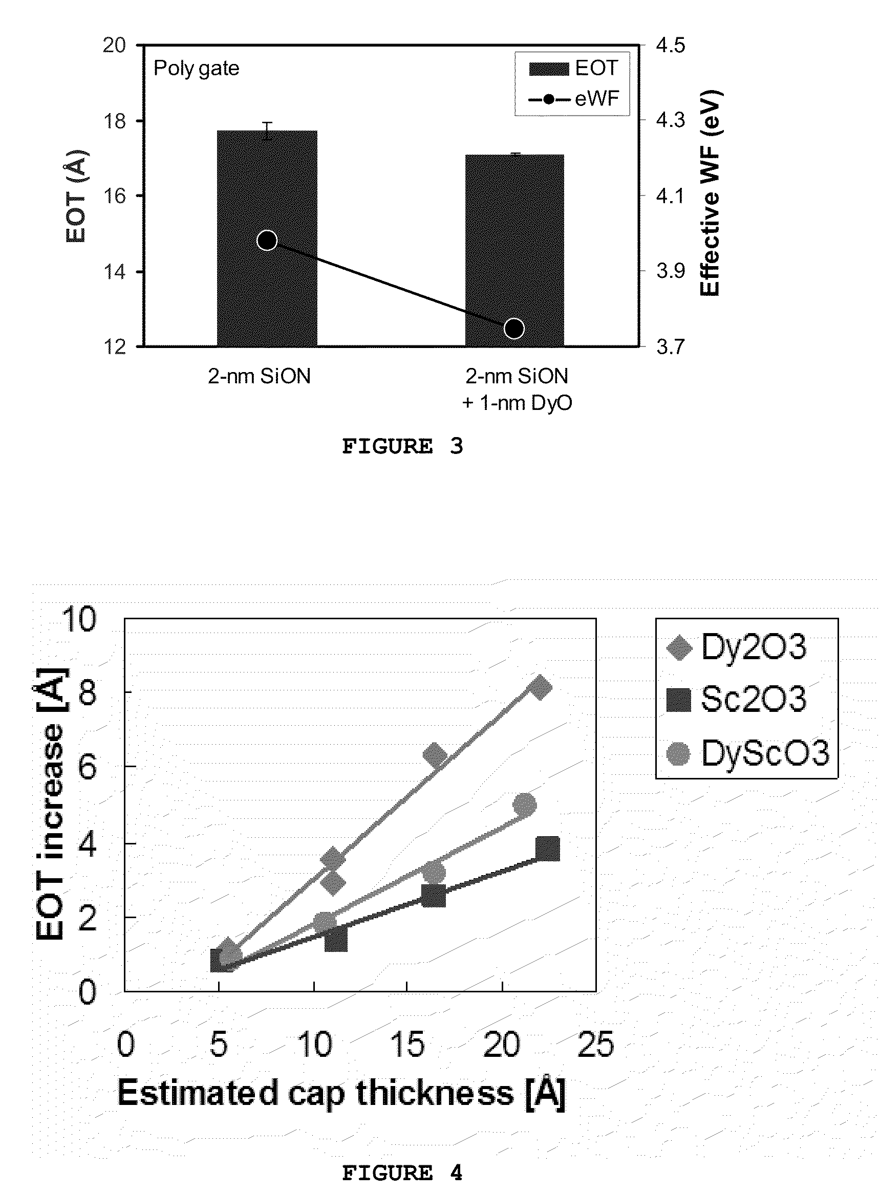
[0059]In one embodiment of the first aspect of the present invention the dielectric capping layer has a thickness smaller than 2 nm, preferably smaller than 1.5 nm and even more preferably smaller than 1 nm and comprises Scandium (Sc) based materials, e.g. Sc oxides, Sc-silicates, or combinations thereof.
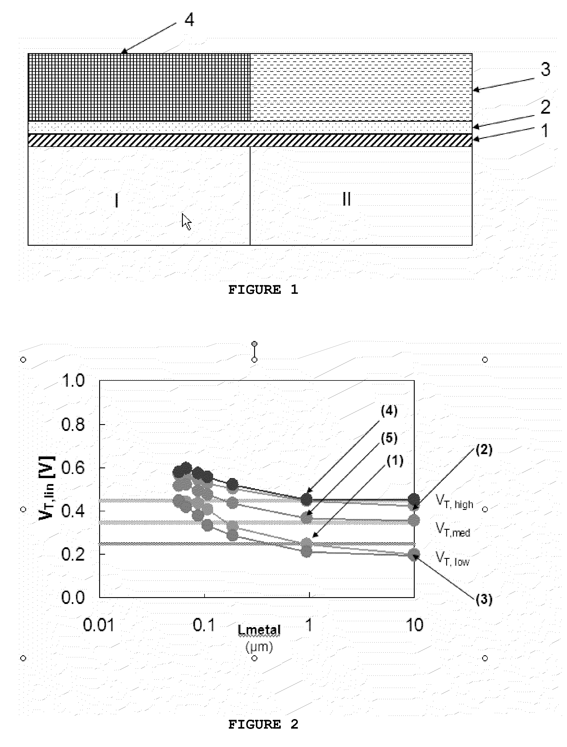
[0060]The high-k dielectric layer (1) can be, for example, selected from the group consisting of SiON, HfSiOx, HfO2, ZrO2 and mixtures thereof. These can present the advantage of a stable, high quality dielectric barrier between the gate electrode, and the channel region of the semiconductor structures forming the semiconductor device.
[0061]The substrate can, for example, comprise Si, Silicon-On-Insulator (SOI), Ge, Germanium on Insulator (GeOI), III-V materials or combinations thereof. The III-V ma...
PUM
 Abstract
Description
Claims
Application Information