Electrophotographic photoconductor, preparation method thereof, electrophotographic apparatus and process cartridge

a photoconductor and electrophotography technology, applied in the field of electrophotographic apparatus and process cartridges, can solve the problems of increasing print costs or power consumption, inability to reduce environmental burdens, and techniques bearing inherent defects to achieve the effect of reducing environmental burdens, high mechanical strength, and satisfying photosensitivity properties

Inactive Publication Date: 2008-03-11
RICOH KK
View PDF71 Cites 19 Cited by
  • Summary
  • Abstract
  • Description
  • Claims
  • Application Information

AI Technical Summary

Benefits of technology

[0017]Accordingly, an object of the present invention is to provide a photoconductor exhibiting high abrasion resistance so as to reduce the exchange frequency of the photoconductor in an electrophotographic apparatus. Such a photoconductor contributes to energy saving in the electrophotographic apparatus, as well as to source saving, energy saving and reduction of environmental pollution in the life cycle of the photoconductor. Another object of the present invention is to provide a photoconductor having satisfactory releasability to thereby provide a long-life image-forming engine with less damages on photoconductor contact-carrying members around the photoconductor. Yet another object of the present invention is to provide a photoconductor that can be prepared at low cost, has low initial cost, can be distributed widely into the market and has a low print cost per one print.

Problems solved by technology

If photoconductors have increased production cost, and / or electrophotographic apparatuses further require a drum heater and other means which have been inherently unnecessary and thereby have increased print cost or have increased power consumption in order to achieve the above objects, such photoconductors and electrophotographic apparatuses cannot gain market acceptance.
These techniques bearing inherent defects cannot contribute to reduction of environmental burdens.
This is because the total environmental burdens cannot be reduced unless products exhibiting high environmental performance are widely used.
The photoconductor, however, used in the electrophotographic apparatus cannot have a prolonged life by merely improving the stress resistance.
Such a photoconductor exhibiting low abrasion may often invite image lag and local image blur due to cleaning failure or invite image blur over an entire face of image-formable region due to filming of toner component onto the surface of the photoconductor.

Method used


Image

  • Electrophotographic photoconductor, preparation method thereof, electrophotographic apparatus and process cartridge
  • Electrophotographic photoconductor, preparation method thereof, electrophotographic apparatus and process cartridge
  • Electrophotographic photoconductor, preparation method thereof, electrophotographic apparatus and process cartridge

Examples


example 1

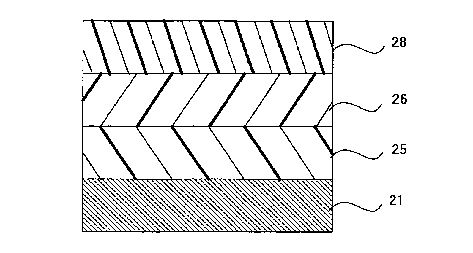
[0407]The following coating composition for a undercoat layer, coating composition for a charge generation layer, coating composition for a charge transport layer were sequentially applied and dried to form an undercoat layer 3 μm thick, a charge generation layer 0.3 μm thick and a charge transport layer 20 μm thick on an aluminum drum having a wall thickness of 0.8 mm and a diameter of 30 mm. Next, a coating composition for a surface top layer was applied to the charge transport layer by spray coating to form a surface top layer 0.95 μm thick. Thus, an electrophotographic photoconductor according to the present invention was prepared.

[0408]

[Coating Composition for Undercoat Layer]Alkyd resin (Beckolite M6401-50, available from 12 parts by weightDainippon Ink and Chemicals Inc.)Melamine resin (Super Beckamine G-821-60, available 8 parts by weightfrom Dainippon Ink and Chemicals Inc.)Titanium oxide (CR-EL, available from Ishihara Sangyo 40 parts by weightKaisha, Ltd.)Methyl ethyl ket...

example 2

[0440]The following coating composition for a undercoat layer, coating composition for a charge generation layer, coating composition for a charge transport layer were sequentially applied and dried to form an undercoat layer 3.5 μm thick, a charge generation layer 0.4 μm thick and a charge transport layer 20 μm thick on an aluminum drum having a wall thickness of 0.8 mm and a diameter of 100 mm. Next, a coating composition for a surface top layer was applied to the charge transport layer by spray coating to form a surface top layer 2 μm thick. Thus, an electrophotographic photoconductor according to the present invention was prepared.

[0441]

[Coating Composition for Undercoat Layer]Alkyd resin (Beckosol 1307-60-EL, available from 10 parts by weightDainippon Ink and Chemicals Inc.)Melamine resin (Super Beckamine G-821-60, available 7 parts by weightfrom Dainippon Ink and Chemicals Inc.)Titanium oxide (CR-EL, available from Ishihara Sangyo 40 parts by weightKaisha, Ltd.)Methyl ethyl ke...

example 3

[0444]An electrophotographic photoconductor was prepared by the procedure of Example 2, except for using the following coating composition for a surface top layer, repeating the coating procedure of the coating composition a total of eight times to give a surface top layer 8 μm thick.

[0445]

[Coating Composition for Photoconductor Surface Top Layer]Crosslinkable charge transporting material 5 parts by weighthaving the following structure and containingreactive hydroxyl groupsThermosetting surfactant (Modiper F200, 10 parts by weightavailable from NOF Corporation)(solid content: 3parts by weight)Thermosetting resin monomer (melamine resin) 12 parts by weight(Super Beckamine L-145-60, available from(solid content: 7.2Dainippon Ink and Chemicals Inc.)parts by weight)Tetrahydrofuran190 parts by weightCyclohexanone 53 parts by weight

[0446]The applied coating composition for a surface top layer was cured at 170° C. for 30 minutes. No endothermic peak was observed in a DSC curve of the resul...


PUM

PropertyMeasurementUnit
light transmittanceaaaaaaaaaa
surface free energyaaaaaaaaaa

Abstract

An electrophotographic photoconductor includes an electroconductive substrate, a photoconductive layer arranged over the electroconductive layer with or without the interposition of an undercoat layer, and a surface top layer containing a crosslinkable resin arranged over the photoconductive layer, the photoconductive layer includes a charge generation layer containing a charge generating material, and a charge transport layer containing a charge transporting material, in which the surface top layer is substantially free from hydroxyl groups and residual uncured portions.

Description

BACKGROUND OF THE INVENTION[0001]1. Field of the Invention[0002]The present invention relates to an electrophotographic photoconductor for use in electrophotographic image forming apparatuses such as copying machines, facsimile machines, laser-beam printers and direct digital (computer-to-plate) plate making machines. The present invention also relates to a method for preparing the photoconductor, and an image forming apparatus and a process cartridge using the electrophotographic photoconductor.[0003]2. Description of the Related Art[0004]Photoconductive materials for use in electrophotographic apparatuses such as copying machines and laser-beam printers have changed from inorganic photoconductive materials such as selenium, zinc oxide and cadmium sulfide to organic photoconductive materials (OPCs). This is because organic photoconductive materials are friendly to environment and have low manufacturing costs and good designing flexibility.[0005]Organic photoconductors are broadly c...

Claims


Application Information

Patent Timeline
Patent Type & Authority Patents(United States)
IPC IPC(8): G03G15/04G03G5/147G03G5/047G03G5/05G03G5/06G03G5/07G03G5/14
CPCG03G5/0575G03G5/0592G03G5/0614G03G5/0616G03G5/0668G03G5/0679G03G5/14708G03G5/14769G03G5/14791G03G5/14795G03G5/06147
Inventor KAMI, HIDETOSHITODA, NAOHIROKAWASAKI, YOSHIAKIKONDO, MAIKOKITAJIMA, RYOICHIKOJIMA, NARIHITONAGAME, HIROSHI
Owner RICOH KK
Why Eureka
Try Eureka