Display device and method of manufacturing same

Inactive Publication Date: 2008-03-11
PANASONIC CORP
View PDF13 Cites 85 Cited by
  • Summary
  • Abstract
  • Description
  • Claims
  • Application Information

AI Technical Summary

Benefits of technology

[0016]In view of the foregoing and other problems, it is an object of the present invention to provide a display device and a method of manufacturi

Problems solved by technology

For this reason, operating power is constantly required for the display operation, and images cannot be displayed in a non-powered state.
Likewise, organic EL elements utilize light emission caused in a state where electric current or voltage is applied to display images, and therefore, the image display is impossible in a non-powered state, as with the TN liquid crystal display elements.
Specifically, when the particles travel in a solution having a large viscosity, their traveling velocity becomes slow, and the display speed (response speed) of the element is accordingly slow.
This increases cost.
Consequently, such an aggregation phenomenon becomes a cause of display image quality degra

Method used


Image

  • Display device and method of manufacturing same
  • Display device and method of manufacturing same
  • Display device and method of manufacturing same

Examples


first preferred embodiment

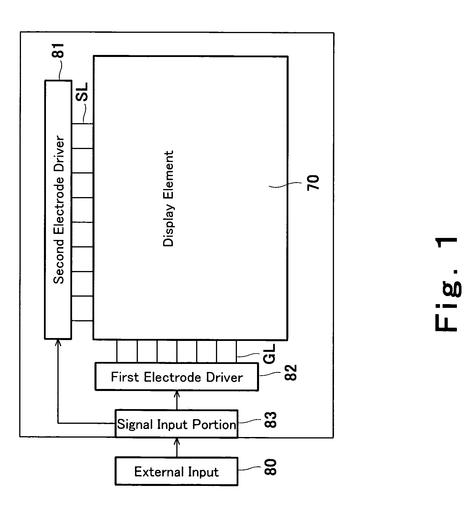
[0102]FIG. 1 is a schematic view showing a display device according to a first preferred embodiment of the present invention. FIGS. 2A to 2C are schematic views showing the configuration of a pixel that constitutes a display element of the display device shown in FIG. 1, which show its cross sections perpendicular to the display screen (hereafter, referred to as “vertical cross sections”).

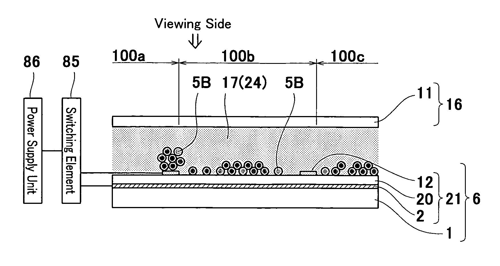
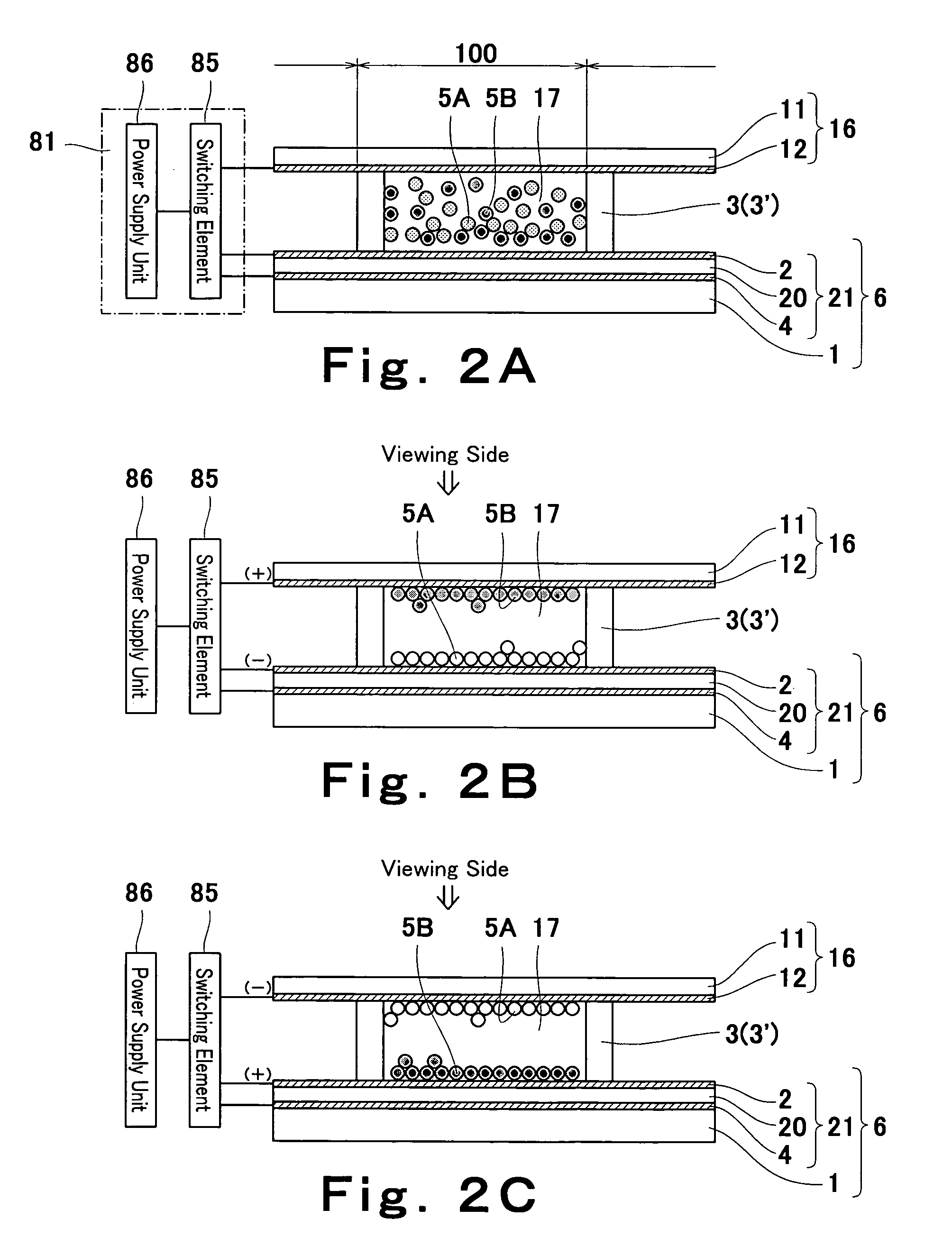
[0103]As shown in FIGS. 1 and 2A to 2C, the display portion of the display device is composed of a display element 70, which is a display panel. The display element 70 has, as shown in FIGS. 2A to 2C, a lower substrate 6 and an upper substrate 16, and the substrates 6 and 16 are opposed to each other by being supported by a spacer 3′ to have a desired gap distance. Thereby, a space 17 is formed between the substrates 6 and 16. The space 17 is partitioned by the spacer 3′, and thus, the spacer 3′ is referred to as a partition wall 3 herein. Each individual region of the space 17 partitioned by the p...

example

[0138]This Example specifically discusses a method of manufacturing a display element according to the present embodiment. Herein, 1.1 mm thick glass substrates are used for the first and second substrates 1 and 11. First, serving as a second electrode 12, an ITO film, which is a light-transmissive, conductive material, is formed on one of the surfaces of a glass substrate that is a second substrate 11. Then, after washing the glass substrate having the ITO film formed thereon, a polycarbonate thin film which has a high hardness is formed on the ITO film. Then, polycarbonate is dissolved in tetrahydrofuran, whereby a 2-5 μm thick insulating film composed of polycarbonate is formed. Here, it is more ideal that the terminal group of the polycarbonate is modified to improve adhesiveness with ITO. In the manner as described above, a upper substrate 16 is produced, in which the second electrode 12 and the insulating film (not shown) are formed on the second substrate 11.

[0139]Meanwhile, ...

second preferred embodiment

[0146]FIG. 3 is a schematic cross-sectional view showing the configuration of a pixel that constitutes a display element of a display device according to a second preferred embodiment of the present invention. As shown in FIG. 3, a display element of the present embodiment has a similar configuration to that of the display element of the first preferred embodiment but differs therefrom in that the black particles 5B has conductivity and that an electron transport layer 7 serving as a charge transport layer is formed on the first and second electrodes 2 and 12.

[0147]Although the first preferred embodiment has discussed a case in which both the colored particles have an insulative property, one kind of the particles may be conductive insofar as at least one kind of the particles is insulative. When the colored particles are conductive, it is necessary to form a thin film containing a charge transport material or an insulative film on the surfaces of the first and second electrodes 2 a...


PUM


Abstract

A lower substrate including a first electrode and an upper substrate including a second electrode are opposed to each other. Partitioned spaces between the two substrates correspond to pixels, each including negatively charged black particles and positively charged white particles. In the lower substrate, a piezoelectric material is sandwiched between a third electrode and the first electrode, thereby forming a vibration-generating portion. In a display operation, a signal voltage corresponding to an image signal is applied between the first and second electrodes, and thus, the black particles and the white particles travel between the electrodes and adhere to the respective electrode surfaces to perform the display operation. Before rewriting the display, a sine wave voltage is applied between the first electrode and the third electrode to cause the vibration-generating portion to generate vibration. Aggregated particles are dissociated, and particles adhering to the electrode are detached, by the vibration.

Description

FIELD OF THE INVENTION[0001]The present invention relates to display devices that can be written and rewritten repeatedly and that are furnished with a display element that performs display operations by causing a plurality of colored particles to travel between a pair of opposing substrates by an electric field. The invention also relates to methods of manufacturing such devices.BACKGROUND OF THE INVENTION[0002]Conventionally, twisted nematic liquid crystal (hereafter referred to as “TN liquid crystal”) display elements and organic electroluminescence (hereafter referred to as “organic EL”) elements have been known to be thin, low power display elements that can be used in personal digital assistants. In TN liquid crystal display elements, the alignment state of liquid crystal molecules in the liquid crystal layer changes only during the period in which a voltage is applied, by which the transmissivity of light that transmits through the liquid crystal layer is controlled to perfor...

Claims


Application Information

Patent Timeline
IPC IPC(8): G09G3/04G02F1/1343G02F1/167G02F1/1679G09G3/34
CPCG02F1/167G09G3/344G09G3/3446G09G2310/061G09G2300/04G09G2300/0434G09G3/3493G02F1/1679G02F1/1343
Inventor OUE, TOSHIYASUYAMAKITA, HIROYUKIKAWAGURI, MARIKO
Owner PANASONIC CORP
Why Eureka
Try Eureka