Techniques for sequentially transferring data from a memory device through a parallel interface

a technology of parallel interface and data transfer, which is applied in the direction of electric digital data processing, instruments, computing, etc., can solve the problem of slow data transfer from the flash device to the fpga

Inactive Publication Date: 2008-03-11
ALTERA CORP
View PDF27 Cites 8 Cited by
  • Summary
  • Abstract
  • Description
  • Claims
  • Application Information

AI Technical Summary

Benefits of technology

[0010]The present invention provides techniques for synchronously transmitting data in parallel from a memory device to a destination circuit using a sequential read mode. The present invention eliminates

Problems solved by technology

Because each set of data bits needs to be individually addressed by the

Method used


Image

  • Techniques for sequentially transferring data from a memory device through a parallel interface
  • Techniques for sequentially transferring data from a memory device through a parallel interface
  • Techniques for sequentially transferring data from a memory device through a parallel interface

Examples


Embodiment Construction

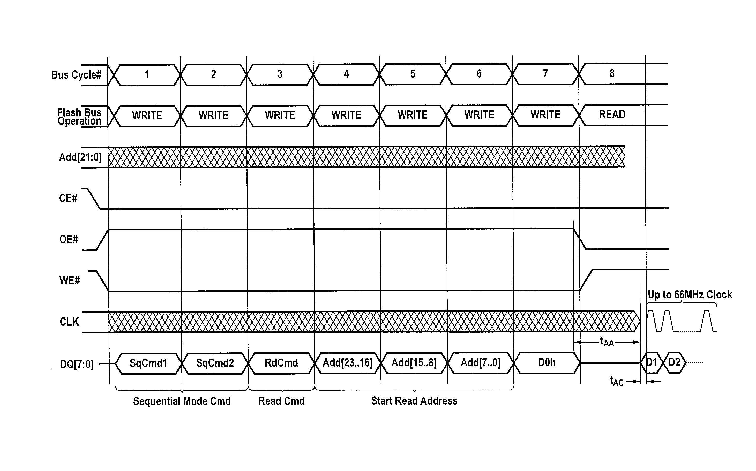
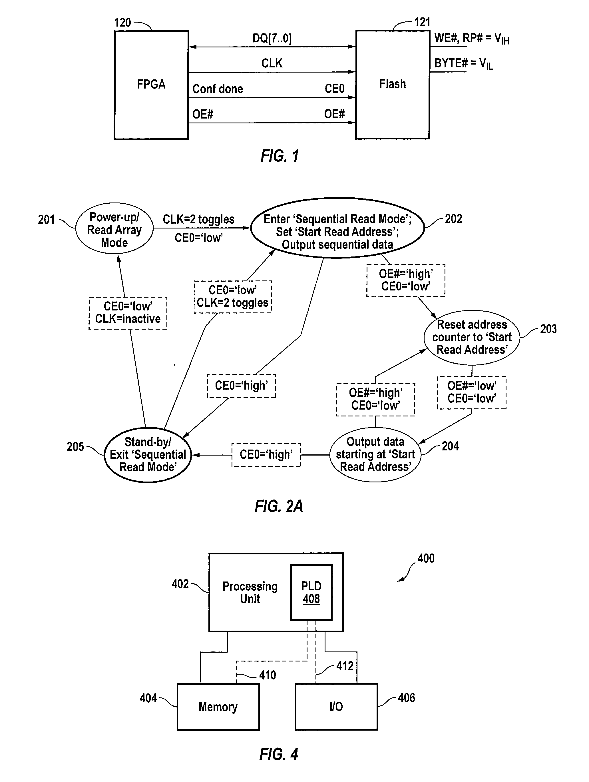
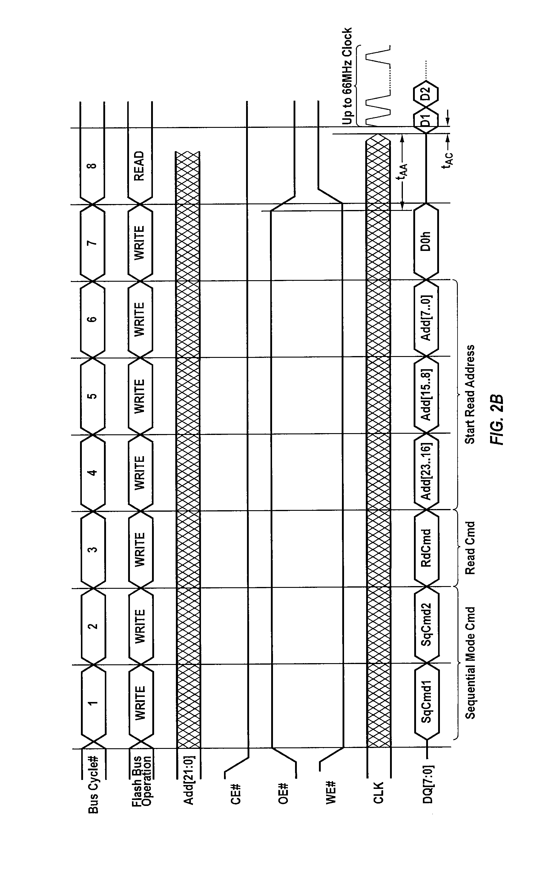
[0020]The present invention provides techniques for synchronously transferring data in parallel from an external memory device to a destination circuit in a sequential read mode.

[0021]The destination circuit can be a programmable integrated circuit such as a field programmable gate array (FPGA), a programmable logic device (PLD), a programmable logic array (PLA), a configurable logic array, etc. The destination circuit can also be an application specification integrated circuit (ASIC), or an ASIC / FPGA hybrid. Although the present invention is discussed primarily in the context of an FPGA as the destination circuit, it should be understood that the destination circuit can be any suitable integrated circuit and that FPGAs are discussed herein merely as an example of the present invention.

[0022]Data is transferred to the destination circuit from an external memory device such as a FLASH or EEPROM memory device. Although the present invention is discussed primarily in the context of FLA...


PUM


Abstract

Techniques are provided for synchronously transmitting data in parallel from an external memory device to a destination circuit using a sequential read mode. The memory device includes an address counter. The address counter generates sequential read addresses for the data bits stored in the memory device. The destination circuit generates a clock signal that controls the address counter. The destination circuit can also transmit a start address to the memory device. The address counter sequentially generates a new read address in response to transitions in the clock signal beginning with the start address. Data bits are transferred in parallel from the memory device to the destination circuit.

Description

BACKGROUND OF THE INVENTION[0001]The present invention relates to techniques for transmitting data from a memory device through a parallel interface, and more particularly, to techniques for transmitting data from a memory device using a parallel sequential read mode.[0002]Programmable integrated circuits such as field programmable gate arrays (FPGAs) are configured (i.e., programmed) using configuration data. Configuration data used to configure a programmable circuit can be stored in an external memory device such as a FLASH memory device.[0003]Configuration data can be transferred in serial or in parallel from a FLASH memory device to an FPGA. For parallel data transfer, some types of prior art FPGAs interface directly with the FLASH memory device using 35 input / output (IO) pins on the FPGA.[0004]The FPGA interfaces directly with the FLASH memory using Asynchronous Read Mode. In this scenario, 23 address pins are provided by the FPGA. In addition to the 23 address pins, 8 data pi...

Claims


Application Information

Patent Timeline
IPC IPC(8): G06F12/00G06F13/00
CPCG06F13/4243
Inventor JOYCE, JUJUMANSUR, DANJEFFERSON, DAVIDZHANG, CHANGSONGLIN, YI-WEN
Owner ALTERA CORP
Why Eureka
Try Eureka