Tray transfer unit and automatic test handler having the same

a transfer unit and automatic technology, applied in the direction of individual semiconductor device testing, coupling device connection, instruments, etc., can solve the problems of double device fault, double device fault, and disadvantages of conventional automatic test handler, so as to reduce product damage resulting from the effect of transferring uni

Inactive Publication Date: 2008-03-25
SAMSUNG ELECTRONICS CO LTD
View PDF27 Cites 12 Cited by
  • Summary
  • Abstract
  • Description
  • Claims
  • Application Information

AI Technical Summary

Benefits of technology

[0015]The present invention is directed to an improved tray transfer unit, and an automatic test handler including such a t

Problems solved by technology

The conventional automatic test handler, however, has disadvantages.
For example, a so-called double device fault may occur during the test process.
A double device fault refers to a fault where two or more semiconductor devices are placed in a single pocket or receptacle of the tray.
A double device fault may result from the malfunction of an adsorption component, e.g., a vacuum adsorptive pad or a vacuum pump, or from the malfunction of a component used to detect the adsorption of the semiconductor device, e.g., a sensor.
If such a fault is caused by the malfunction of a component related to vacuum, it may be that a vacuum adsorptive force was not properly applied through the vacuum adsorptive pad or was improperly released.
In such instances, the semiconductor device may not be adsorbed for loading or unloading, or may be released prematurely during transfer.
If the fault is caused

Method used


Image

  • Tray transfer unit and automatic test handler having the same
  • Tray transfer unit and automatic test handler having the same
  • Tray transfer unit and automatic test handler having the same

Examples


Embodiment Construction

[0040]Exemplary embodiments of the present invention will be described below with reference to the accompanying drawings.

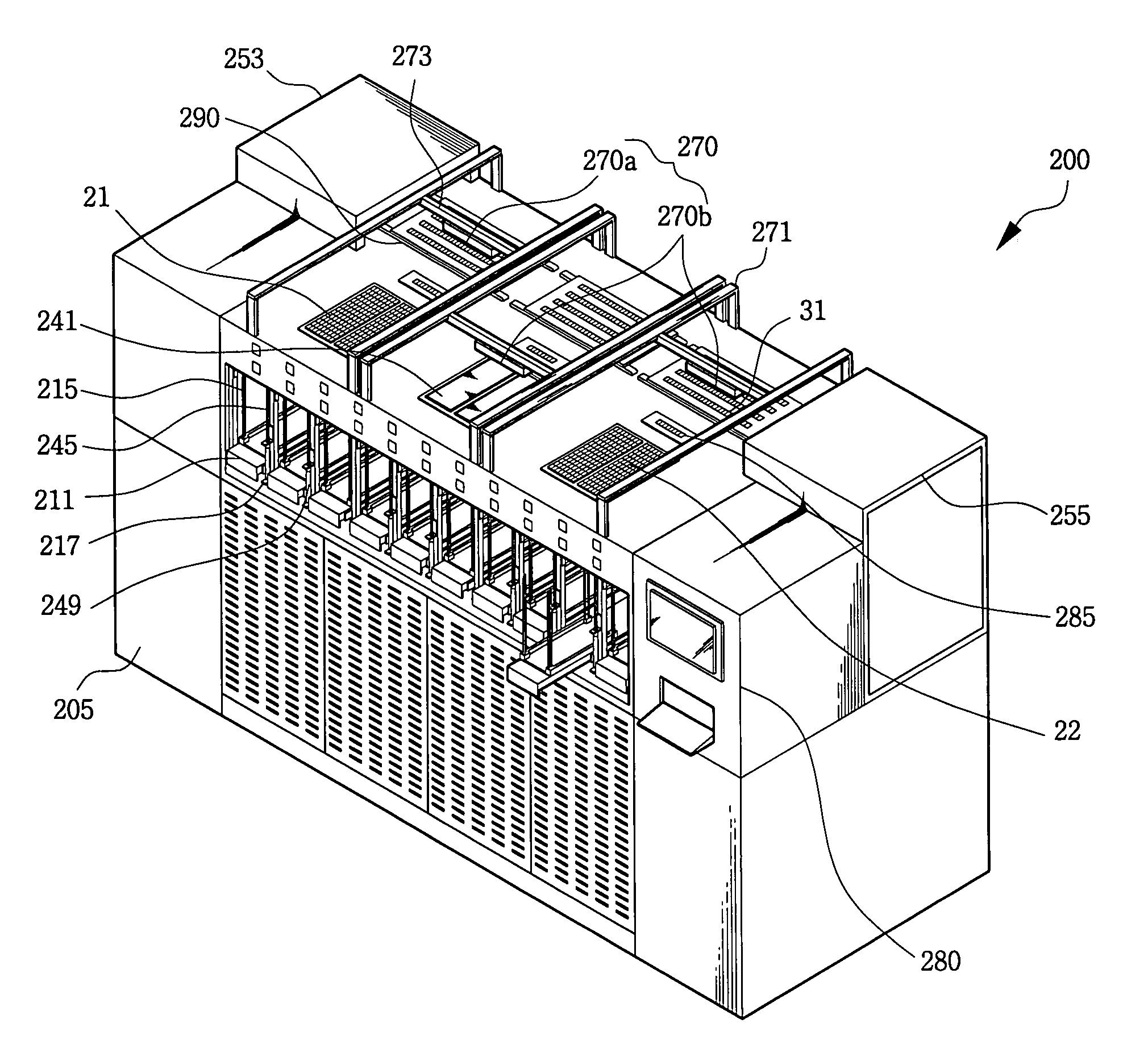
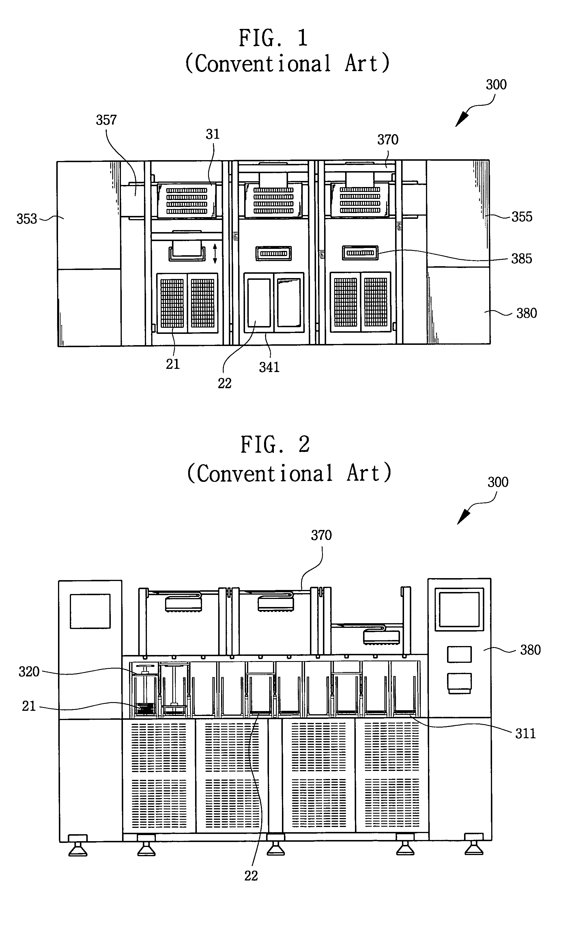
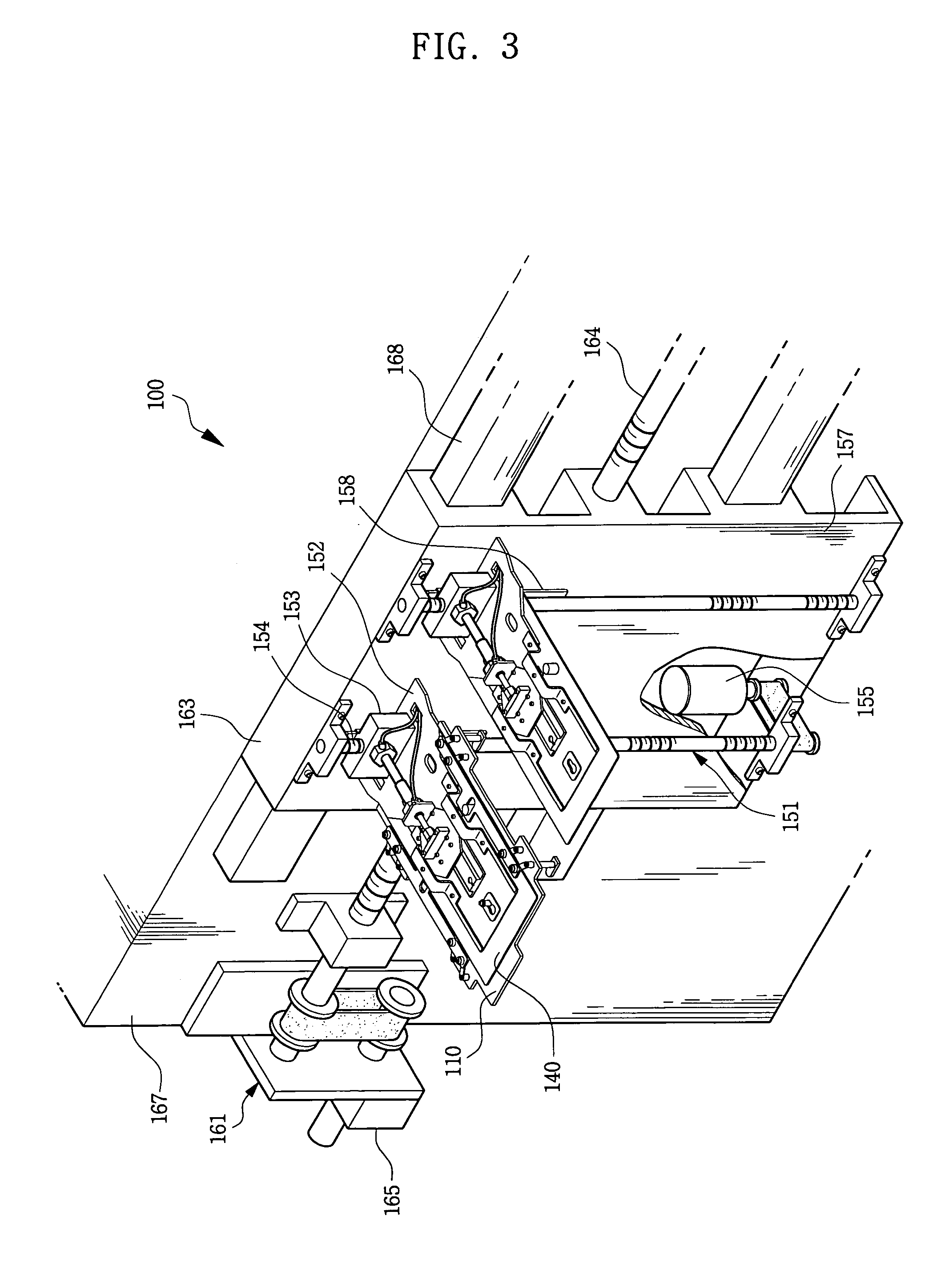
[0041]Referring to FIGS. 3 through 9, a tray transfer unit 100 comprises a transfer plate 110, detecting switches 130, a detecting substrate 140 and a driving unit including both a vertical driving unit 151 and a horizontal driving unit 161. The transfer plate 110 supports a tray containing semiconductor devices placed in an array of pockets provided on the tray. The driving units 151 and 161 may be utilized to transfer and position the transfer plate 110 relative to a tray that is intended for transfer.

[0042]The transfer plate 110 has connection holes 112 located at the edges thereof, as shown in FIG. 5. Tray holders 120 are formed at the connection holes 112 for supporting the tray. A series of installation holes 113 are provided on the transfer plate 110 at locations corresponding to each pocket 25 of the tray 21 that will be transferred by the transfer plate. ...


PUM


Abstract

Provided is a tray transfer apparatus having a transfer plate arranged and configured to support a tray containing a number of semiconductor devices in an array of pockets. The tray transfer apparatus further includes a driving means arranged and configured for the movement and positioning of the transfer plate. The transfer plate is provided with a plurality of tray holders that may be selectively engaged to support a tray and with detecting means corresponding to the array of pockets provided in a supported tray. In instances in which one or more of the detecting means sense the presence of more than one semiconductor device in a corresponding pocket of a supported tray, the tray transfer apparatus will generate an alarm signal and/or suspend operation so that corrective measures may be taken.

Description

CROSS REFERENCE TO RELATED APPLICATIONS[0001]This U.S. non-provisional application claims priority under 35 U.S.C. § 119 to Korean Patent Application No. 2003-36411 filed Jun. 5, 2003, the contents of which are incorporated herein, in its entirety, by reference.BACKGROUND OF THE INVENTION[0002]1. Field of the Invention[0003]The present invention relates to a semiconductor manufacturing apparatus and, in particular, to an improved tray transfer unit and an automatic test handler including such a tray transfer unit.[0004]2. Description of the Related Art[0005]After being sawed from a wafer, semiconductor devices are typically placed in trays during certain points during their manufacture to reduce the likelihood of damage and to increase the ease with which the semiconductor devices may be handled. The semiconductor devices are typically removed from a tray for processing and discharged to the same or a different tray after processing in a manner that maintains the order in which they...

Claims


Application Information

Patent Timeline
IPC IPC(8): G01R31/28G01R31/26H01L21/00H01L21/673H01L21/677H01L21/68
CPCG01R31/2893H01L21/67259H01L21/67333H01L21/68
Inventor LEE, EUN-SOO
Owner SAMSUNG ELECTRONICS CO LTD
Why Eureka
Try Eureka