Optoelectronic circuit board with optical waveguide and optical backplane

a technology of optoelectronic circuit boards and backplanes, applied in the direction of optical waveguide light guides, optical elements, instruments, etc., can solve the problems of wire-attributable delays and emis, line waveguides, and difficulty in aligning optical axes, etc., to achieve high speed/operation flexibility

Inactive Publication Date: 2008-03-25
CANON KK
View PDF21 Cites 2 Cited by
  • Summary
  • Abstract
  • Description
  • Claims
  • Application Information

AI Technical Summary

Benefits of technology

[0007]An optical transmission device according to the invention comprises an optical transmission medium and a plurality of optical receivers, and the optical transmission medium has a linear line waveguide. At least one of the optical receivers is adapted to receive a first optical signal propagated through the line waveguide, while at least one of the optical receivers is adapted to receive a second optical signal propagated through the optical transmission medium. The optical transmission medium is typically a sheet-shaped two-dimensional optical waveguide. However, it may alternatively be a three-dimensional optical transmission medium, which may be cubic or spherical. Since a two-dimensional or three-dimensional optical transmission medium and a linear line waveguide are arranged in a mixed state in the above arrangement, it is possible to realize an optical transmission device that is adapted for high speed / operation with flexibility and is structurally compact.
[0010]It may be so arranged that the line waveguide is made to show a complex refractive index greater than that of the non-line section of the optical transmission medium, which is the part thereof other than the line waveguide, so that light being propagated in parallel with the part is guided and propagated with priority. The difference of the complex refractive indexes is preferably not greater than 1%, more preferably not greater than 0.5%, when light being propagated through the entire optical transmission medium passes through the line waveguide, so as to reduce the influence thereof (in other words, so as to reduce the loss and the refraction when light being propagated through the non-line section strikes the line waveguide and is transmitted through it).
[0011]The ½-th power of the cross sectional area of the line waveguide is preferably not greater than ¼, more preferably not greater than ⅛, of the thickness of the sheet-shaped optical transmission medium so as to be able to prevent light being propagated through the optical transmission medium from being coupled to the line waveguide.
[0015]Such an optoelectronic circuit according to the invention may comprise an optical transmission device according to the invention and an electric wiring layer that are laid one on the other so that it is free from problems including signal delays of electric wiring and EMIs and adapted to raise the degree of design freedom as circuit board.

Problems solved by technology

However, as the processing speed rises, there arise various problems including wire-attributable delays and EMIs (electromagnetic interferences).
Therefore, the use of such a line waveguide is accompanied by a number of problems including the need of using a large number of optical switches, the difficulty of aligning optical axes, the need of micro-processing the optical waveguide, the use of a large number of parts and the difficulty of preparation if an enhanced degree of freedom for wiring and alteration of an optical circuit is to be desired.
However, the information processing apparatus disclosed in the above U.S. patent document is not satisfactory in terms of the degree of freedom for optical wiring.

Method used


Image

  • Optoelectronic circuit board with optical waveguide and optical backplane
  • Optoelectronic circuit board with optical waveguide and optical backplane
  • Optoelectronic circuit board with optical waveguide and optical backplane

Examples


example 1

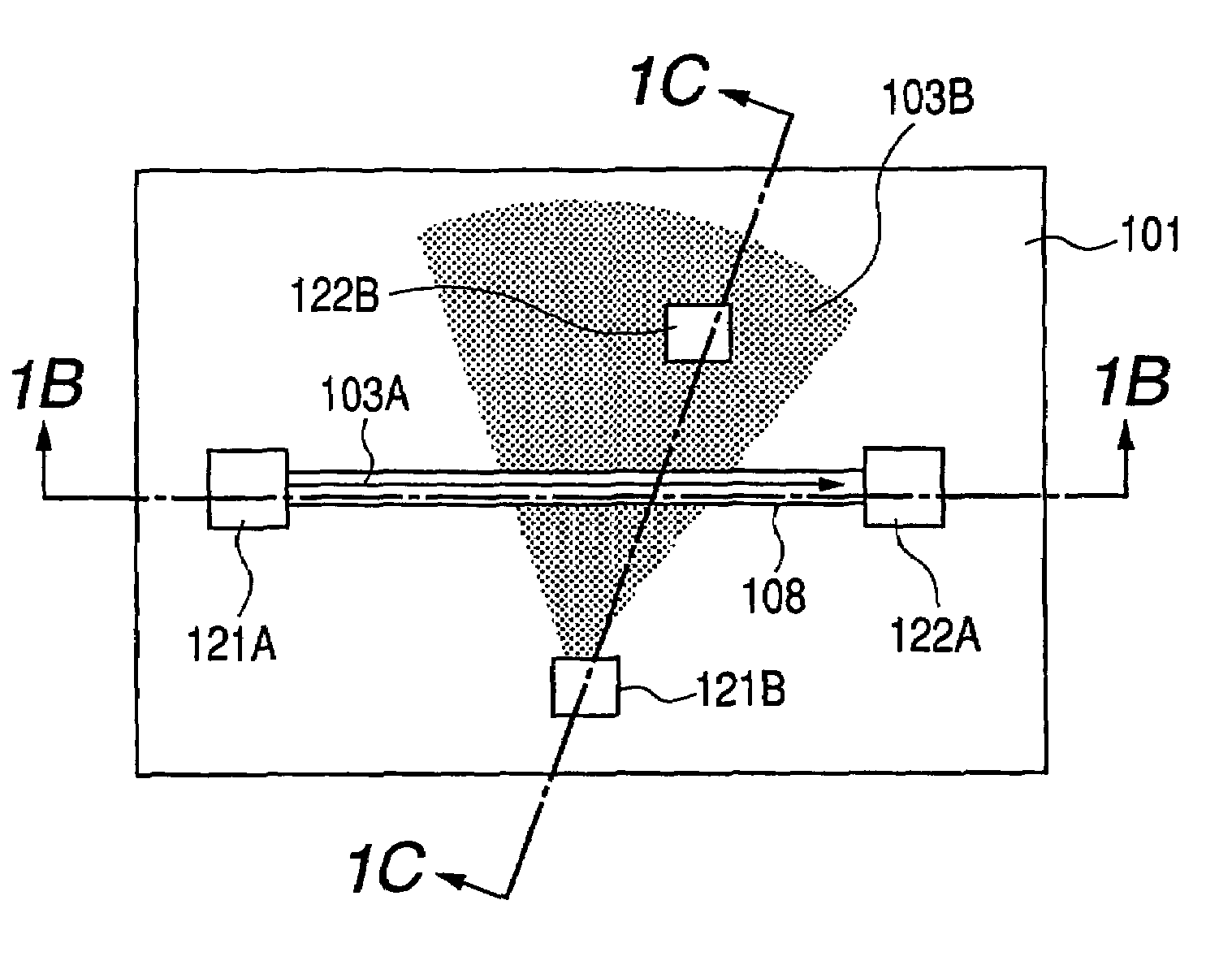
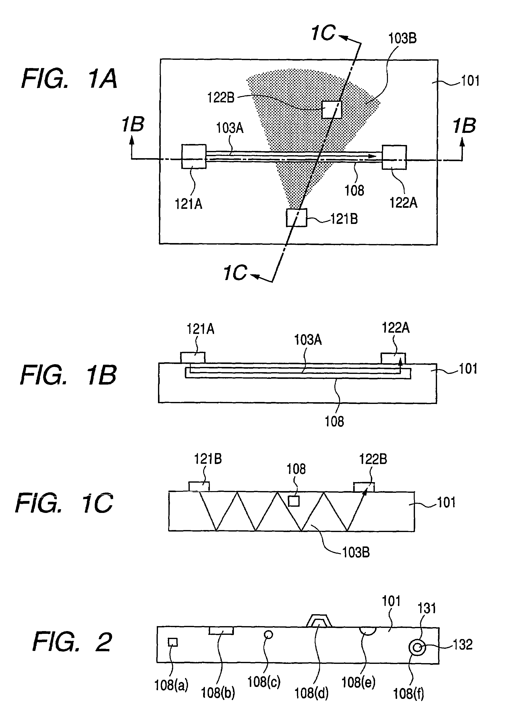
[0064]In Example 1, an optical transmission device having a configuration similar to that of FIGS. 1A through 1C is prepared. In this example, the optical transmission medium 101 is made of fluorinated polyimide (refractive index: about 1.55) and has dimensions of 3 cm×5 cm. A single linear line waveguide 108 is buried so as to run horizontally in the optical transmission medium 101 as shown in FIGS. 1A through 1C. The line waveguide 108 shows a square cross section like that of 108(a) in FIG. 2 and each of the sides is about 25 microns long.

[0065]The refractive index of the line waveguide 108 is greater than that of the surrounding non-line section by about 1%. While both the line waveguide and the non-line section are made of fluorinated polyimide, their refractive indexes can be differentiated by differentiating the respective fluorine contents. The illustrated structure is formed by forming a film layer of fluorinated polyimide that makes the non-line section on a substrate, sub...

example 2

[0071]In Example 2, an optical transmission device having a configuration similar to that of FIGS. 4A and 4B is prepared. FIGS. 4A and 4B show plan views of the same arrangement. In this example, the optical transmission medium 101 is made of PMMA (refractive index: about 1.49) and optical fibers of quartz of a single mode are buried in the optical transmission medium 101 for line waveguides 108. The optical fibers show a cross section similar to that of 108(f) in FIG. 2. Thus, the cores 132 of the optical fibers operate as line waveguides 108 and the clad sections 131 of the optical fibers and the surrounding PMMA operate as non-line section.

[0072]The cores and the clad sections of the optical fibers show respective diameters of about 10 μm and about 125 μm and a relative refractive index of 0.2%. Since the optical transmission medium 101, or the PMMA layer, has a thickness of 200 μm, it can be used as a multi-mode two-dimensional optical waveguide, whereas the line waveguides 108 ...

example 3

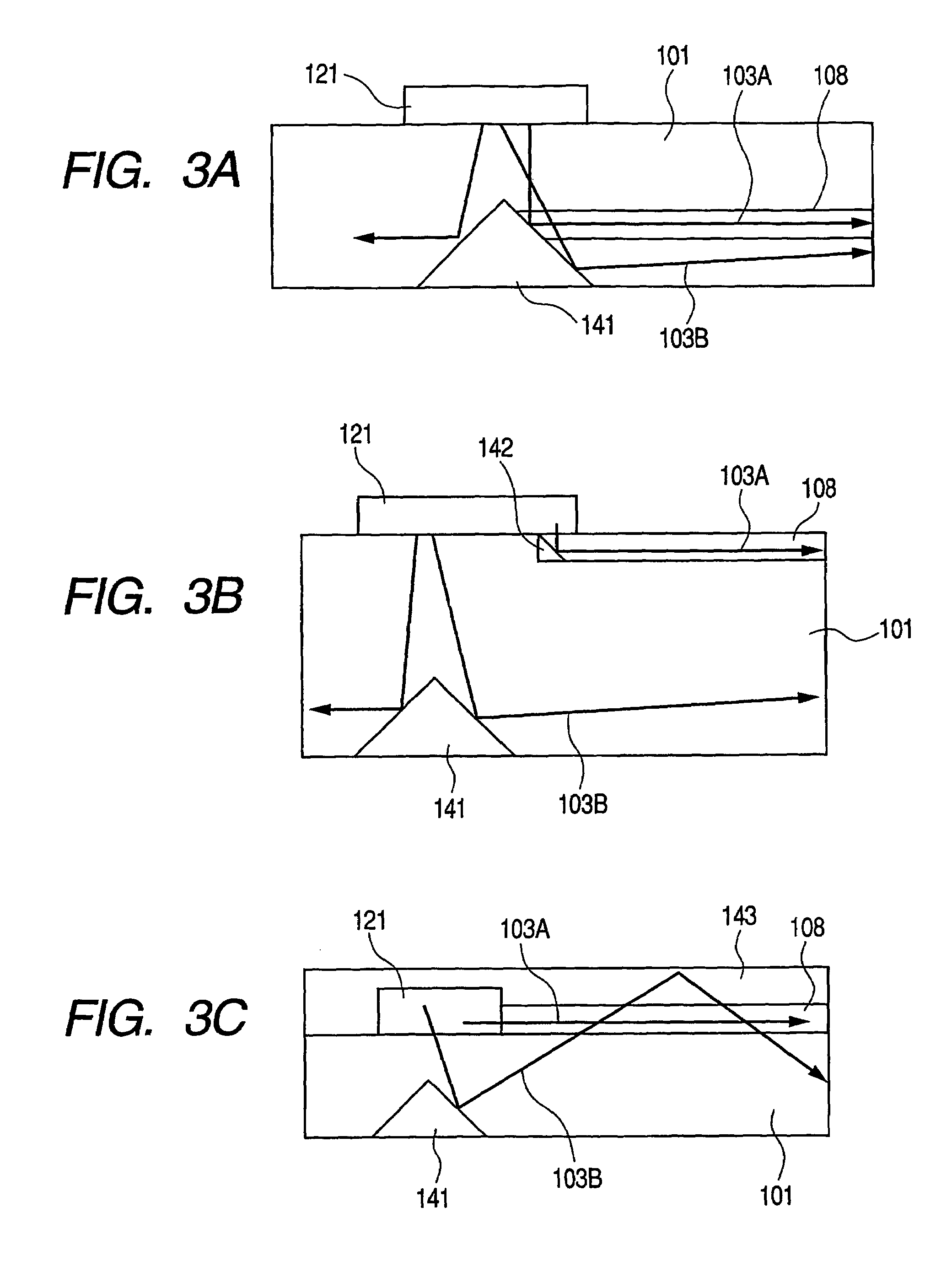
[0079]In Example 3, an optical transmission device having a configuration similar to that of FIG. 5 is prepared. An optical transmission medium 101 having a configuration similar to that of its counterpart of Example 1 is also used in this example. In this example, the optical transmission medium 101 has a size of 3 cm square and is provided with optical ports 102 adapted to transmit and receive data signals by way of a plurality of line waveguides 108. A parallel transmission can be conducted between the ports that are linked together by way of a plurality of line waveguides 108. Apart from these ports, the optical transmission device additionally comprises a broadcast port 123 for broadcasting a clock signal. The optical signal 103B from the broadcast port 123 is propagated through the optical transmission medium that is a two-dimensional waveguide and received by the other ports 102.

[0080]Each of the ports 102 comprises an optical transmitter adapted to output light to the corres...


PUM


Abstract

An optical transmission device comprises an optical transmission medium and a plurality of optical receivers, and the optical transmission medium has a linear line waveguide. At least one of the optical receivers is adapted to receive a first optical signal propagated through the line waveguide, while at least one of the optical receivers is adapted to receive a second optical signal propagated through the optical transmission medium.

Description

TECHNICAL FIELD[0001]The present invention relates to an optical transmission device including a two-dimensional (2D) or three-dimensional (3D) optical transmission medium and a line waveguide and also to an optoelectronic circuit including such an optical transmission device and thereby comprising a mixture of electronic circuits and optical circuits.BACKGROUND ART[0002]In recent years, information processing instruments such as personal computers, mobile phones and PDAs (personal digital assistants) have been required to show a high processing speed in addition to be compact and lightweight. However, as the processing speed rises, there arise various problems including wire-attributable delays and EMIs (electromagnetic interferences).[0003]Proposed techniques for avoiding wire-attributable delays and EMIs include the use of an optical wire or a line waveguide (U.S. Pat. No. 5,357,122).[0004]Optical wires provide advantages including high speed transmission capabilities and being i...

Claims


Application Information

Patent Timeline
Patent Type & Authority Patents(United States)
IPC IPC(8): G02B6/12G02B6/122G02B6/42G02B6/43H04B10/25H04B10/272H04B10/80
CPCG02B6/4214G02B6/4246G02B6/43H01L2224/16225H01L2924/15192
Inventor IWASAKI, TATSUYA
Owner CANON KK
Why Eureka
Try Eureka