Semiconductor storage device and semiconductor integrated circuit
a technology of semiconductor integrated circuit and storage device, which is applied in the direction of semiconductor devices, solid-state devices, instruments, etc., can solve the problems of preventing higher integration, and achieve the effects of reducing device area, product yield improvement, and reducing manufacturing costs
- Summary
- Abstract
- Description
- Claims
- Application Information
AI Technical Summary
Benefits of technology
Problems solved by technology
Method used
Image

Examples
first embodiment
[0111]This embodiment is explained as follows with reference to FIGS. 1 to 5.
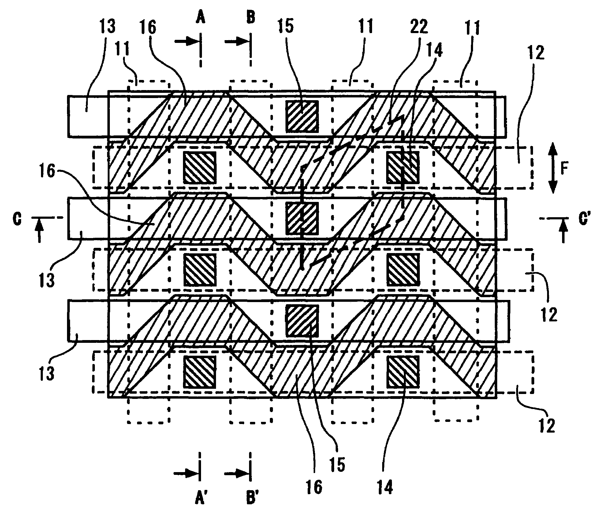
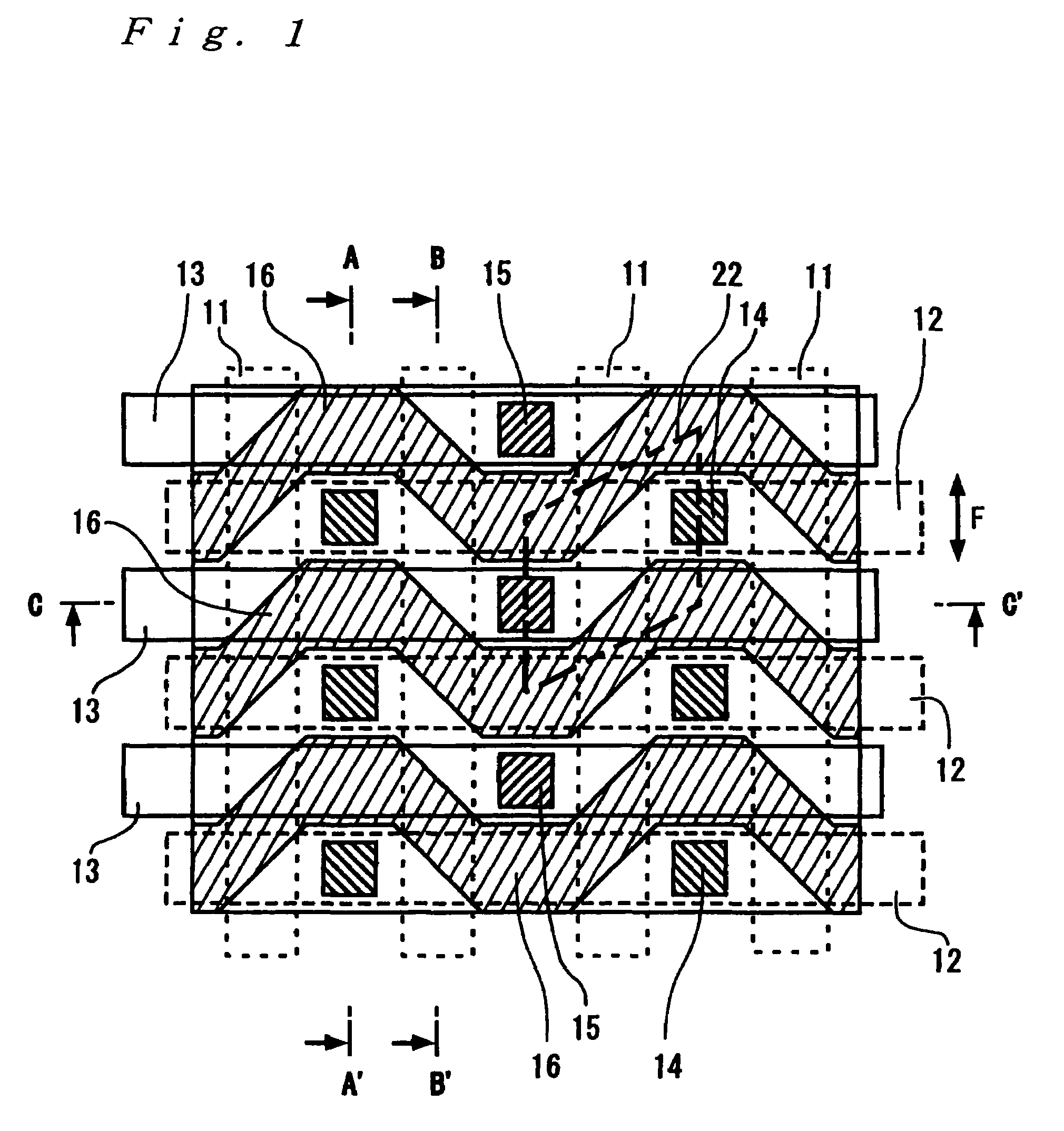
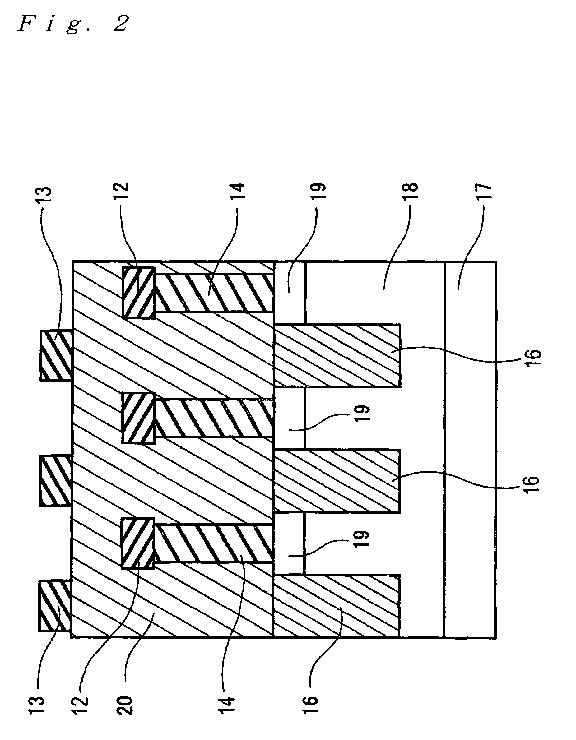
[0112]FIGS. 1 to 4 are schematic views of a memory cell array which is a semiconductor storage device that forms this embodiment. FIG. 1 is a schematic view thereof. FIG. 2 is a sectional view as taken along the cut-plane line A-A′ of FIG. 1, FIG. 3 is a sectional view as taken along the cut-plane line B-B′ of FIG. 1, and FIG. 4 is a sectional view as taken along the cut-plane line C-C′ of FIG. 1. FIG. 5 is a circuit diagram of a memory cell array which is the semiconductor storage device that forms the first embodiment of the invention.
[0113]First, constitution of the semiconductor storage device of this embodiment is explained with reference to FIGS. 1 to 4. As can be seen from FIGS. 2 to 4, a P-type well region 18 is formed in a silicon substrate 17. Further, a plurality of device isolation regions 16 are formed so as to meander and extend in the lateral direction of FIG. 1 (respective meandering band re...
second embodiment
[0128]This embodiment is described below with reference to FIGS. 6 and 7.
[0129]The structure of the semiconductor storage device of this embodiment differs from the semiconductor storage device of the foregoing first embodiment only in the structure of the well region. FIG. 6 is a sectional view as taken along the cut-plane line B-B′ of FIG. 1. An N-type deep well region 25 and a P-type shallow well region 26 are formed in a silicon substrate 17. This well region 26 is partitioned into a plurality by device isolation regions 16. The device isolation regions 16 are set to such a depth that both-side P-type shallow well regions 26 sandwiching a device isolation region 16 are electrically isolated from each other. Each of the partitioned well regions 26 extends meandering in the lateral direction in FIG. 1 as in the first embodiment. These partitioned well regions 26, as described next, serve as third bit lines, respectively.
[0130]Next, circuit construction of this embodiment is explai...
second-b embodiment
[0145]This embodiment is explained below with reference to FIG. 9. The structure of the semiconductor storage device of this embodiment differs from the semiconductor storage device of the foregoing second embodiment in that a charge-trapping film 34 is used instead of the floating gate (FIG. 9). On the circuit diagram, the case is absolutely the same with the second embodiment (FIG. 7).
[0146]In this embodiment, it is implementable to perform selective write and selective erase operations for memory cells using the charge-trapping film instead of the floating gate, for the same reasons as described in the foregoing second-a embodiment. In this case, the charge-trapping film is, for example, Si3N4 / SiO2 film, SiO2 / Si3N4 / SiO2 film (ONO film) and devices using this are exemplified by, for example, MNOS, SNOS and SONOS. Although silicon nitride is expressed as Si3N4 and silicon oxide as SiO2, yet their component ratios are not limited by these expressions. Also, ferroelectric memory film...
PUM
 Abstract
Description
Claims
Application Information
 - R&D Engineer
- R&D Manager
- IP Professional
- Industry Leading Data Capabilities
- Powerful AI technology
- Patent DNA Extraction
Browse by: Latest US Patents, China's latest patents, Technical Efficacy Thesaurus, Application Domain, Technology Topic.
© 2024 PatSnap. All rights reserved.Legal|Privacy policy|Modern Slavery Act Transparency Statement|Sitemap