Interface circuit, power conversion device, and vehicle-mounted electric machinery system

a technology of power conversion device and interface circuit, which is applied in the direction of logic circuit coupling/interface arrangement, dynamo-electric converter control, pulse technique, etc., can solve the problems of large power consumption, narrow operating temperature range, and optical isolators, and achieve high noise tolerance, high reliability, and reliable transmission

Inactive Publication Date: 2008-04-01
HITACHI LTD
View PDF12 Cites 47 Cited by
  • Summary
  • Abstract
  • Description
  • Claims
  • Application Information

AI Technical Summary

Benefits of technology

[0014]In accordance with the invention, signals can be reliably transmitted even when there is fluctuation in the potential difference in reference potentials between circuits transmitting signals to each other. Thus, the invention can provide a highly noise-tolerant, highly reliable, and highly heat-resistant interface circuit.

Problems solved by technology

Optical isolators, however, consumes large amounts of power, deteriorate greatly with age, and have a narrow operating temperature range.
Furthermore, optical isolators cannot be formed on a silicon substrate as an integrated circuit (IC) and must be mounted on a printed-circuit board as an externally attached component when it is mounted within a vehicle-mounted inverter.
However, in the conventional interface circuits, no consideration has been given to the fact that the reference potential difference between the circuits between which signal transmission is carried out is subject to large variation due to the influence of noise or the like.

Method used


Image

  • Interface circuit, power conversion device, and vehicle-mounted electric machinery system
  • Interface circuit, power conversion device, and vehicle-mounted electric machinery system
  • Interface circuit, power conversion device, and vehicle-mounted electric machinery system

Examples


embodiment 2

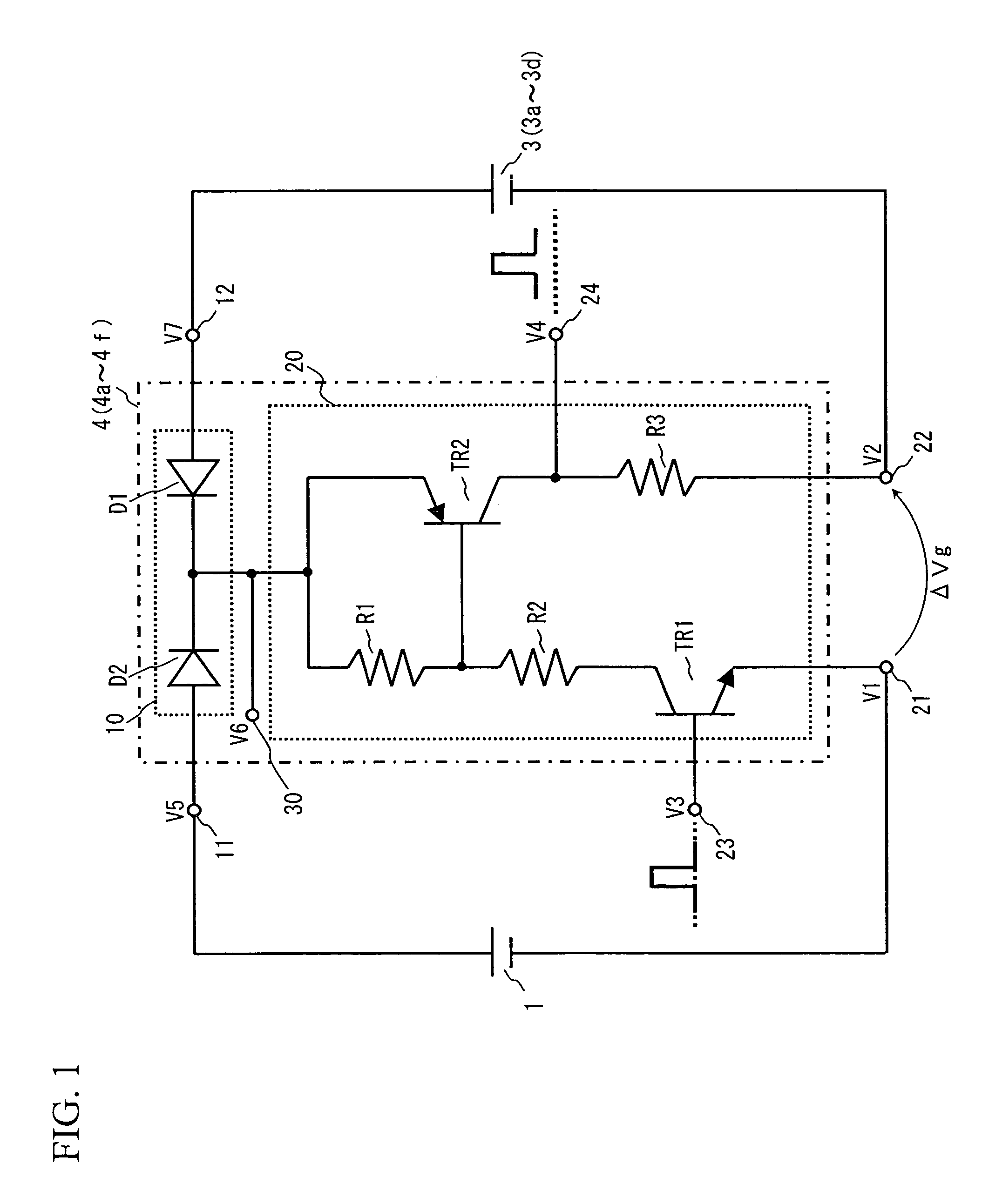
[0192]A second embodiment of the invention will be described with reference to FIG. 7.

[0193]FIG. 7 shows the circuit configuration of driving interface circuits 7 (u-phase, v-phase, and w-phase upper-arm driving interface circuits 7a, 7b, and 7c and u-phase, v-phase, and w-phase lower-arm driving interface circuits 7d, 7e, and 7f).

[0194]The present embodiment is a variation of the first embodiment and differs therefrom in the configuration of the potential selection circuit. Other portions are identical to those of the first embodiment.

[0195]While the following description of the present embodiment is made with reference to the driving interface circuits 7, it is possible to configure an abnormality detection interface circuit by exchanging the circuit from the sixth terminal 30 to the first terminal 21 of the level shift circuit 20 (left-side of the circuit shown in FIG. 7) for the circuit from the sixth terminal 30 to the second terminal 22 thereof (right-side of the circuit shown...

embodiment 3

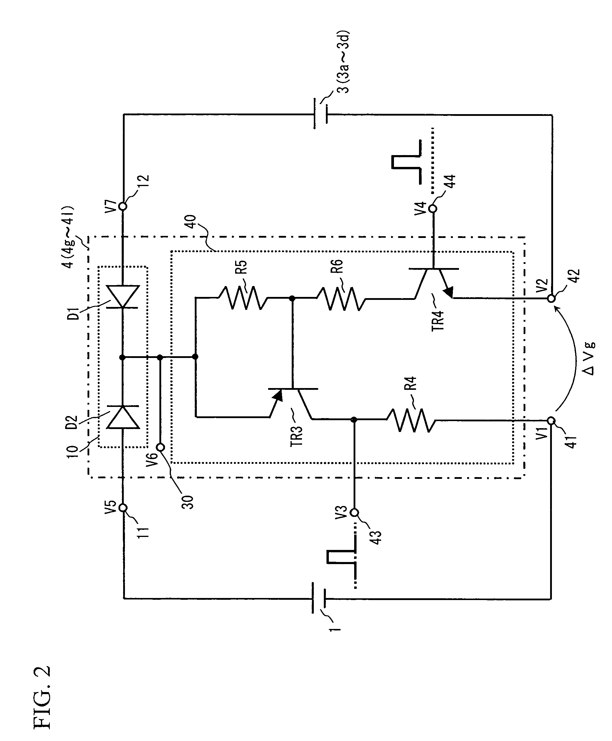
[0204]A third embodiment of the invention will be described with reference to FIG. 8.

[0205]FIG. 8 shows the circuit configuration of driving interface circuits 8 (u-phase, v-phase, and w-phase upper-arm driving interface circuits 8a, 8b, and 8c and u-phase, v-phase, and w-phase lower-arm driving interface circuits 8d, 8e, and 8f) in the present embodiment.

[0206]The present embodiment is a variation of the second embodiment and identical thereto except for the configuration of the potential selection circuit.

[0207]While the following description concerns the circuit configuration of the driving interface circuits 8 as an example, it is possible to configure an abnormality detection interface circuit by exchanging the circuit from the sixth terminal 30 to the first terminal 21 of the level shift circuit 20 (left-side of the circuit shown in FIG. 8) for the circuit from the sixth terminal 30 to the second terminal 22 thereof (right-side of the circuit shown in FIG. 8), as in the second...

embodiment 4

[0216]A fourth embodiment of the invention will be described with reference to FIG. 9.

[0217]FIG. 9 shows the circuit configuration of driving interface circuit 9 (u-phase, v-phase, and w-phase upper-arm driving interface circuits 9a, 9b, and 9c and u-phase, v-phase, and w-phase lower-arm driving interface circuits 9d, 9e, and 9f).

[0218]The foregoing description of the first to third embodiments has been made with reference to the driving interface circuits such that the reference potential of a pulse signal is on the low-potential side of the insulated power supply 1 and a pulse signal that rises with respect to the reference potential is transmitted. In the present embodiment, however, a configuration of the driving interface circuit 9 is described in which unlike the first to third embodiments the reference potential of pulse signal is on the high-potential side of the insulated power supply 1 and a pulse signal that falls with respect to the reference potential is transmitted.

[02...


PUM


Abstract

An interface circuit capable of reliably transmitting signal even when there is fluctuation in the potential difference in reference potentials between circuits between which signal transmission is carried out. An interface circuit 4 is comprised of a level shift circuit 20 and a potential selection circuit 10 for selecting the potential of a power supply voltage for operating the level shift circuit 20. The potential selection circuit 10 selects one of a plurality of input potentials. The level shift circuit 20 receives a voltage pulse having a first potential as reference potential and outputs a voltage pulse having a second potential as reference potential. The level shift circuit 20 is operated on the basis of both a potential difference between the output potential from the potential selection circuit and the first potential and a potential difference between the selected potential and the second potential.

Description

BACKGROUND OF THE INVENTION[0001]1. Field of the Invention[0002]The present invention relates to an interface circuit used for signal transmission between circuits having different reference potentials. It also relates to a power conversion device and a vehicle-mounted electric machinery system.[0003]2. Background Art[0004]An example of conventional interface circuits is disclosed in Patent Document 1. This conventional interface circuit includes a current source and a resistor, wherein a pulse signal inputted from a circuit with a first reference potential is transmitted as a pulse signal having a second reference potential different from the 1st potential by switching the direction of current through the resistor. In this way, signal transmission between circuits with different reference potentials is carried out without employing any externally attached components such as an optical isolator.[0005]Patent Document 1: JP Patent Publication (Kokai) No. 9-46145 A (1997)SUMMARY OF THE...

Claims


Application Information

Patent Timeline
Patent Type & Authority Patents(United States)
IPC IPC(8): H02P1/00B60L9/18H02M1/08H02M7/48H03K17/687H03K19/0175H03K19/082
CPCH03K19/00376H03K19/018F02N2011/0888
Inventor INABA, MASAMITSUIWAMURA, MASAHIROSHIGETA, SATORU
Owner HITACHI LTD
Why Eureka
Try Eureka