Method of IC fabrication, IC mask fabrication and program product therefor

a mask layer and ic technology, applied in the field of integrated circuit manufacturing, can solve the problems of consuming a tremendous amount of computing resources for each layer, affecting the product quality of the mask layer, so as to reduce the ic design to product turn around time

Inactive Publication Date: 2008-04-01
GOOGLE LLC
View PDF8 Cites 222 Cited by
  • Summary
  • Abstract
  • Description
  • Claims
  • Application Information

AI Technical Summary

Benefits of technology

[0008]It is a purpose of the invention to reduce IC design to product turn around time;
[0009]It is another purpose of the invention to reduce the resources consumed in converting an IC physical design into masks;
[0010]It is another purpose of the invention to reduce IC mask dataprep time;
[0011]It is yet another purpose of the invention to reduce the volume of data handled in making IC masks, while reducing dataprep time.

Problems solved by technology

Unfortunately, a typical state of the art IC design may have thousands, millions and perhaps billions of shapes on each layer.
Consequently, proximity correcting all of the shapes on each of the layers can be a daunting task, consuming a tremendous amount of computing resources for each layer, e.g., it may take 440 CPU hours (more than 18 days of dedicated computer time) in a state of the art high performance server.
So, the turnaround time for dataprep of a single such mask layer on a typical state of the art high performance server may be months.
However, using even the most advanced algorithms and the most powerful servers, it may still take more than a CPU week to complete proximity correction for a single chip.
Thus, dataprep on a single design can clog a foundry that is meant to process several chip designs in that week.

Method used


Image

  • Method of IC fabrication, IC mask fabrication and program product therefor
  • Method of IC fabrication, IC mask fabrication and program product therefor
  • Method of IC fabrication, IC mask fabrication and program product therefor

Examples


Embodiment Construction

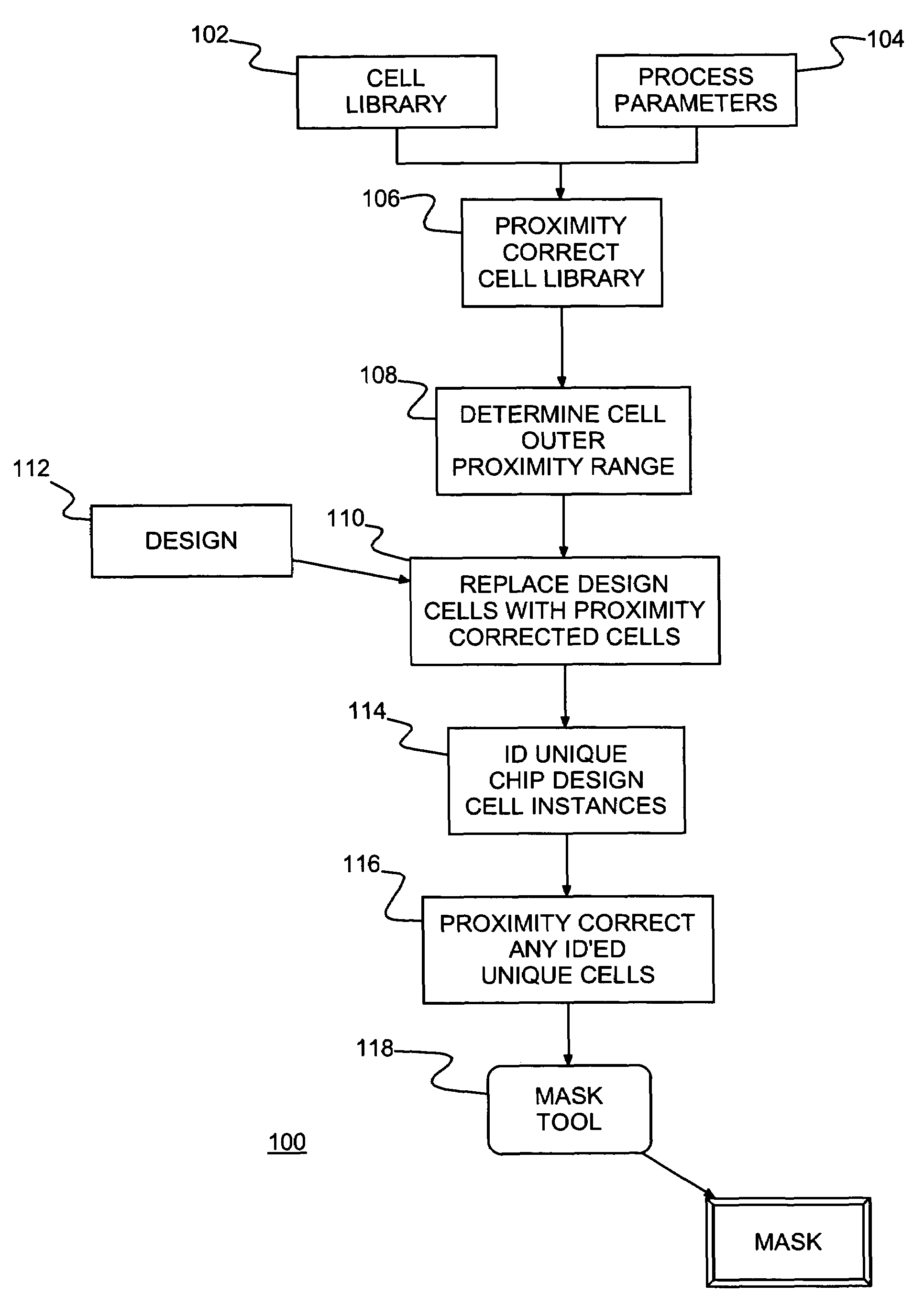
[0018]Turning now to the drawings and, more particularly, FIG. 1 shows a flow diagram example 100 for fabricating integrated circuits (ICs) and, in particular, converting design data for use in a mask making tool (e.g., dataprep) to form mask shapes according to a preferred embodiment of the present invention. The present invention has application to any hierarchical circuit design, whether a fully custom design, a nested design or a design based in standard cell logic. Thus, the design is based on a cell library 102 that, typically, contains physical designs (design layouts) for basic design blocks or books used by a designer in designing an IC chip. For example, the cell library 102 may be a standard cell logic library for standard cell design and, optionally, may also include specially designed blocks / books, macros and etc., e.g., simple and complex logic designed for a particular project or chip design. A process parameter database 104 contains process specific information (e.g....


PUM

PropertyMeasurementUnit
distanceaaaaaaaaaa
critical dimensionaaaaaaaaaa
perimeteraaaaaaaaaa

Abstract

A method of forming integrated circuit (IC) chip shapes and a method and computer program product for converting an IC design to a mask, e.g., for standard cell design. Individual book / macro physical designs (layouts) are proximity corrected before unnesting and an outer proximity range is determined for each proximity corrected physical design. Shapes with a unique design (e.g., in boundary cells and unique instances of books) are tagged and the design is unnested. Only the unique shapes are proximity corrected in the unnested design, which may be used to make a mask for fabricating IC chips / wafers.

Description

CROSS REFERENCE TO RELATED APPLICATION[0001]The present invention is a continuation of U.S. Provisional Patent Application Ser. No. 60 / 574,921, entitled “Method to Reduce Runtime For VLSI Dataprep Operation” to Puneet Gupta et al., filed Feb. 26, 2004, assigned to the assignee of the present invention and incorporated herein by reference.FIELD OF THE INVENTION[0002]The present invention generally relates to integrated circuit manufacturing and more particularly to producing high quality masks for patterning semiconductor layers that define circuit design shapes forming integrated circuits.BACKGROUND DESCRIPTION[0003]A typical integrated circuit (IC) chip is a stack of several levels or sequentially formed layers of shapes. Each layer is stacked or overlaid on a prior layer and patterned (e.g., photolithographically) to define the shapes that combine to form devices (e.g., field effect transistors (FETs)) and connect the devices into circuits. In a typical state of the art complement...

Claims


Application Information

Patent Timeline
Patent Type & Authority Patents(United States)
IPC IPC(8): G06F17/50G03F1/14
CPCG03F1/144G03F1/36
Inventor GUPTA, PUNEETHENG, FOOK-LUENLAVIN, MARK A.
Owner GOOGLE LLC
Why Eureka
Try Eureka