Multichip circuit module and method for the production thereof

a technology of multi-chip circuits and circuit modules, applied in the direction of printed circuit manufacturing, printed circuit aspects, printed circuit non-printed electric components association, etc., can solve the problem of disadvantageous addition of operations, and achieve the effect of avoiding the change of electrical properties

Inactive Publication Date: 2008-04-15
TECH UNIV BRAUNSCHWEIG
View PDF17 Cites 25 Cited by
  • Summary
  • Abstract
  • Description
  • Claims
  • Application Information

AI Technical Summary

Benefits of technology

[0016]It is an object of the invention to provide an improved multichip circuit module with a more compact structure which is less expensive and, at the same time, more highly integrated.
[0024]In comparison with the conventional production methods of multichip circuit modules, the number of operations in the assembly and connecting technique is reduced by using standard technologies. The multichip circuit module may therefore be produced relatively inexpensively and, on account of the cavities, has a more highly integrated, more compact structure.
[0027]The filling material is not intended to fill the interspaces of the cavities completely, in order to prevent wetting of the surface of the semiconductor chip and of the bumps with filling material, so that a change in the electrical properties is avoided as far as possible.

Problems solved by technology

In order to shield the multichip circuit modules, additional operations are disadvantageously required.

Method used


Image

  • Multichip circuit module and method for the production thereof
  • Multichip circuit module and method for the production thereof

Examples


Embodiment Construction

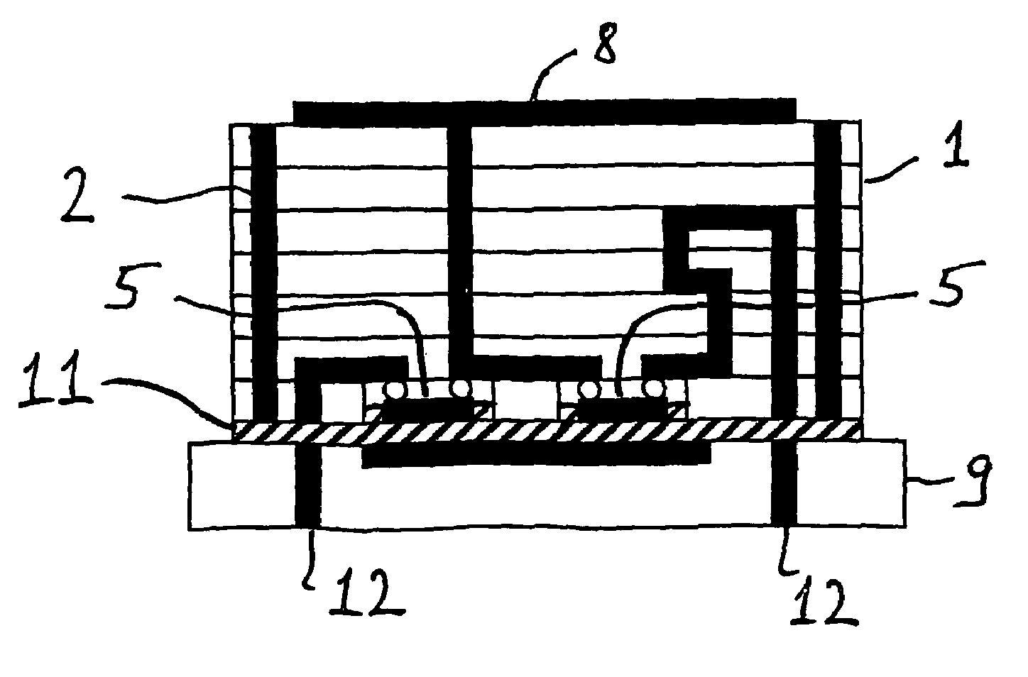
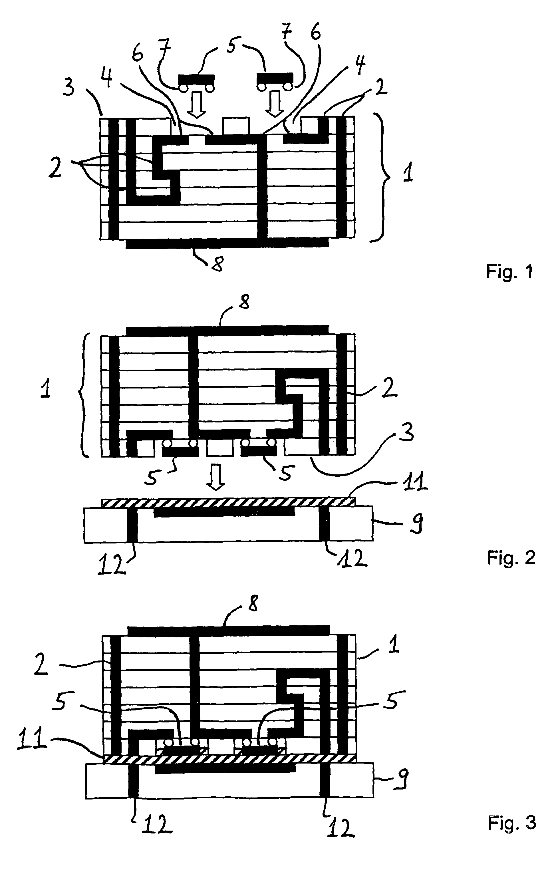
[0032]FIG. 1 reveals a sketch of a multilayer carrier substrate 1 which has a large number of conductor tracks 2. Provided on a mounting surface 3 of the carrier substrate 1 are cavities 4 in the form of rectangular recesses, into which semiconductor chips 5 can be inserted. Provided in the cavities 4 are corresponding connecting contacts 6 for bumps 7 on the underside of the semiconductor chips 5. With the aid of the bumps 7 and the connecting contacts 6, electrical contact can be made with the semiconductor chips 5 in the cavities 4 by the known flip-chip technique. As a cost-effective implementation of multilayer carrier substrates 1, in particular in conjunction with the production of cavities 4, the LTCC (low-temperature co-fired ceramics) technology is recommended.

[0033]Provided on the underside of the carrier substrate 1, which is opposite the mounting surface 3, is a planar antenna arrangement 8, for example a patch antenna. Such a design is now possible, since the carrier s...


PUM


Abstract

A multichip circuit module includes a main board, at least one carrier substrate mounted on and in electrical contact with the main board, and at least one semiconductor chip arranged on the carrier substrate and in electrical contact therewith. The carrier substrate has at least one cavity on an assembly surface for receiving the semiconductor chip. The cavity includes connecting contacts which join with associated bumps on the semiconductor chip using a flip-chip technique. The assembly surface of the carrier substrate is placed on a contact surface of the main board, and a filling material is provided between the contract surface of the main board and the assembly surface of the carrier substrate.

Description

FIELD OF THE INVENTION [0001]The invention relates to a multichip circuit module having a main circuit board, at least one carrier substrate which is mounted on the main circuit board and which is in electrical contact with the main circuit board, and at least one semiconductor chip on the carrier substrate which is in electrical contact with the carrier substrate,[0002]the carrier substrate having at least one cavity on a mounting surface to accommodate at least one semiconductor chip,[0003]connecting contacts for associated bumps of the semiconductor chip being provided in the cavity,[0004]the at least one semiconductor chip being mounted on the connecting contacts by using the bumps in the flip-chip technique,[0005]the mounting surface of the carrier substrate being applied to a contact surface of the main circuit board, a filling material being provided between the contact surface of the main circuit board and the mounting surface of the carrier substrate.[0006]The invention fur...

Claims


Application Information

Patent Timeline
Patent Type & Authority Patents(United States)
IPC IPC(8): H01L23/12H01L23/538H01L23/66H05K1/00H05K1/03H05K1/14H05K1/18H05K3/32
CPCH01L23/5385H01L23/552H01L23/66H05K1/141H01L2223/6677H01L2224/16H01L2924/01078H01L2924/09701H01L2924/15153H01L2924/1517H01L2924/15192H01L2924/1532H01L2924/3025H05K1/0298H05K1/0306H05K1/183H05K3/323H05K2201/10477H05K2201/10674H01L2224/16225H01L2224/16235H01L2224/73253
Inventor HEYEN, JOHANNJACOB, ARNE F.
Owner TECH UNIV BRAUNSCHWEIG
Why Eureka
Try Eureka