Image display apparatus using current-controlled light emitting element

a technology of light emitting element and image display, which is applied in the direction of identification means, instruments, static indicating devices, etc., can solve the problems of difficulty in maintaining high-quality image display, difficulty in displaying high-quality images, and difficulty in realizing large-size and high-definition displays

Inactive Publication Date: 2008-04-15
INNOLUX CORP
View PDF23 Cites 183 Cited by
  • Summary
  • Abstract
  • Description
  • Claims
  • Application Information

AI Technical Summary

Benefits of technology

[0013]It is an object of the present invention to solve at least the problems in the conventional technology.

Problems solved by technology

The former has a simple configuration but has a difficulty in realization of a large-size and high-definition display.
However, when the thin film transistor whose channel layer is formed of amorphous silicon is used as the driver element, there exists a problem such that the conventional image display apparatus as shown in FIG. 9 has a difficulty in keeping high-quality image display over a long period of time.
Therefore, even if the same potential is supplied from the data line 101, the brightness of the organic EL element 105 varies according to variations in the threshold voltage, which makes it difficult to display a high-quality image.
Consequently, the organic EL elements 105 cannot be densely arranged thereon, which causes occurrence of a new problem such that it becomes difficult to perform high-definition image display.

Method used


Image

  • Image display apparatus using current-controlled light emitting element
  • Image display apparatus using current-controlled light emitting element
  • Image display apparatus using current-controlled light emitting element

Examples


first embodiment

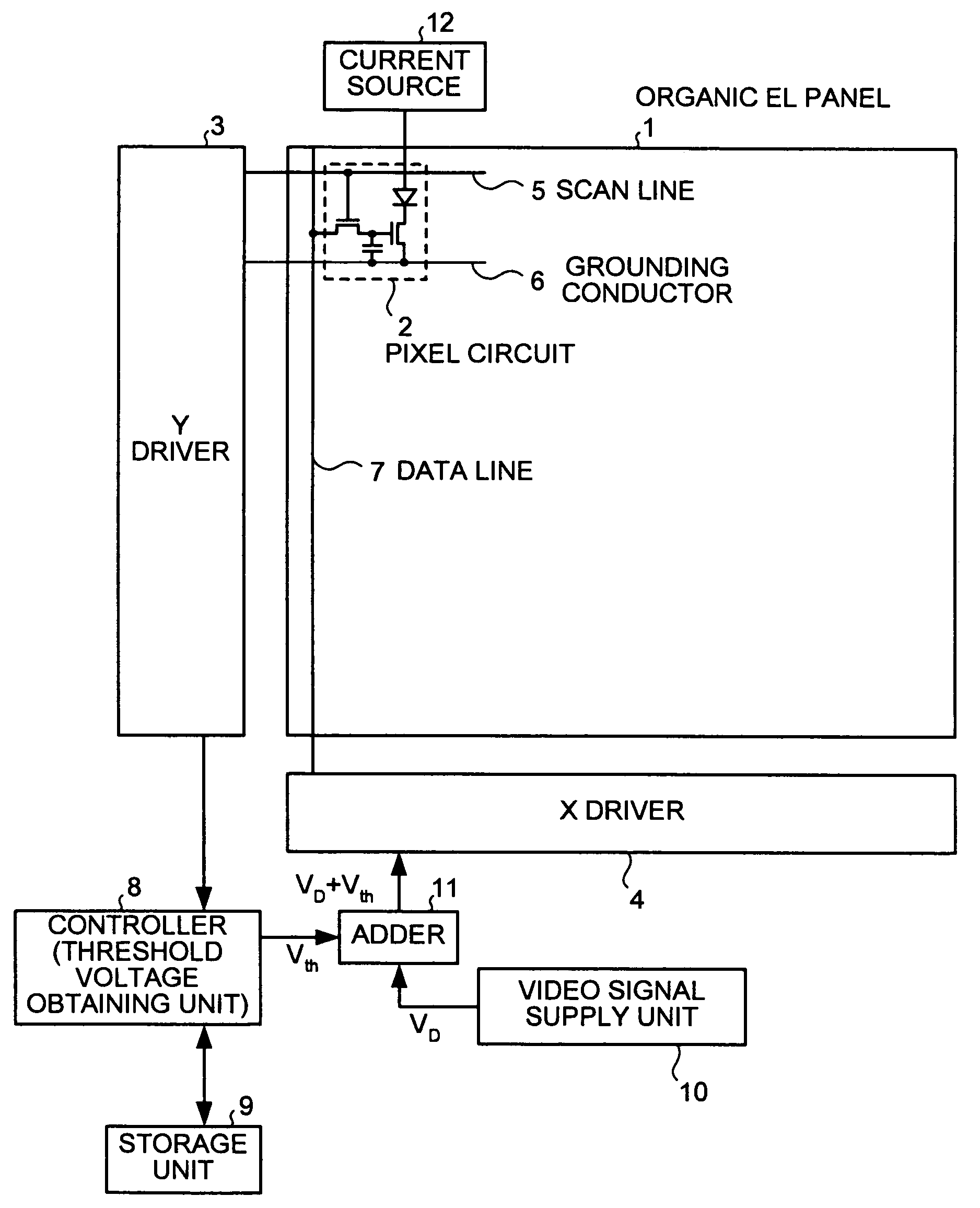
[0026]An image display apparatus according to the present invention is explained below. The image display apparatus is an active matrix image display apparatus using a thin film transistor as a driver element. A gate-source voltage is obtained by a controller so that the driver element is made to be on-state once in a state in which potential control of a grounding conductor that is connected to the driver element is stopped, charge is accumulated in the grounding conductor, and after this, the driver element becomes off-state again. Upon displaying an image, the threshold voltage obtained and a data voltage corresponding to a display brightness are applied to the gate electrode of the driver element to perform image display.

[0027]FIG. 1 is a schematic diagram of the entire configuration of the image display apparatus according to the first embodiment. As shown in FIG. 1, the image display apparatus according to the first embodiment includes an organic EL panel 1 with a large number...

second embodiment

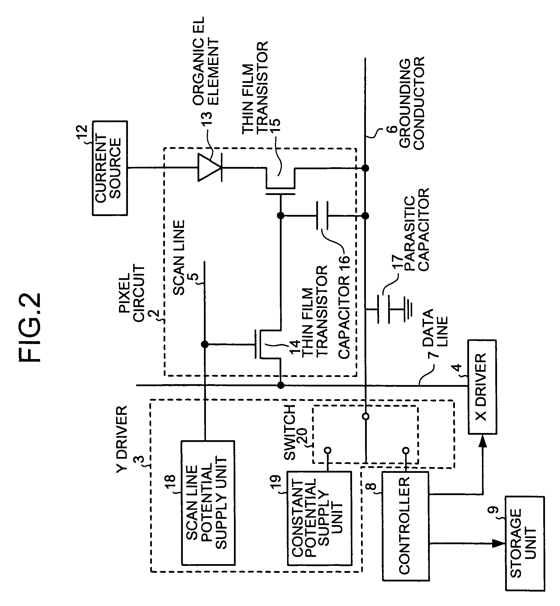
[0057]FIG. 6A to FIG. 6C are diagrams for illustrating process of measuring source electrode potentials of the thin film transistor 15 according to the FIG. 7 is a graph of a variation in source electrode potential of the thin film transistor 15 upon measuring the source electrode potential and of a variation in the gate-source voltage. As shown in FIG. 7, a curve 1, represents a variation in the source electrode potential and a curve 12 represents a variation in the gate-source voltage. Measurement of the source electrode potential is explained below with reference to FIG. 6A to FIG. 6C and FIG. 7.

[0058]As shown in FIG. 6A, a connection destination of the grounding conductor 6 is switched to the controller 8 by the switch 20 to cause the potential of the scan line 5 to rise, and the thin film transistor 14 as the switching element is made to be on-state. The gate electrode of the thin film transistor 15 is provided with a potential Vg supplied from the data line 7 to become on-sta...


PUM


Abstract

A pixel circuit includes a driver element that is supplied with a potential from a data line. The driver element controls a value of current passing through an electric light emitting element. Upon obtaining a threshold voltage, a conductive member connected to the electric light emitting element is made to be a floating state to cause the driver element to become on-state, variations in the potential of the conductive member caused by charges passing through the driver element to flow into the conductive member are detected by a threshold voltage detector to obtain the threshold voltage of the driver element.

Description

BACKGROUND OF THE INVENTION[0001]1) Field of the Invention[0002]The present invention relates to an image display apparatus using a current-controlled light emitting element, and more particularly to an active matrix image display apparatus which controls brightness uniformly across its display unit.[0003]2) Description of the Related Art[0004]An organic electro-luminescence (EL) display apparatus using a self-luminous organic EL element (Organic Light Emitting Diode) does not need a backlight, which is required for a liquid crystal display device. This organic EL display apparatus is therefore suitable for a thin display device, and its practical use as a next generation display device has been expected because of no restriction in a view angle.[0005]An image display apparatus using the organic EL element can employ a simple (passive) matrix type and an active matrix type as a drive system. The former has a simple configuration but has a difficulty in realization of a large-size an...

Claims


Application Information

Patent Timeline
Patent Type & Authority Patents(United States)
IPC IPC(8): G09G3/32G09F9/30H01L51/50G09G3/20G09G3/30G09G5/10H01L27/32H05B33/00H05B33/14
CPCG09G3/3233G09G2300/0842G09G2320/043G09G2320/0285G09G2320/029G09G2320/0233
Inventor ONO, SHINYAKOBAYASHI, YOSHINAO
Owner INNOLUX CORP
Why Eureka
Try Eureka