Data flow scheme for low power DRAM
a data flow and low-power technology, applied in the field of dram memories, can solve the problems of power consumption, many new applications are more and more data-intensive, sense amplifier operation may fail, etc., and achieve the effect of reducing the power consumption of drams
- Summary
- Abstract
- Description
- Claims
- Application Information
AI Technical Summary
Benefits of technology
Problems solved by technology
Method used
Image


Examples
Embodiment Construction
[0024]The preferred embodiments disclose methods and circuits for a DRAM memory having a reduced power consumption by optimizing the pre-charging power of bit lines during read operation and avoiding pre-charging between write operation.
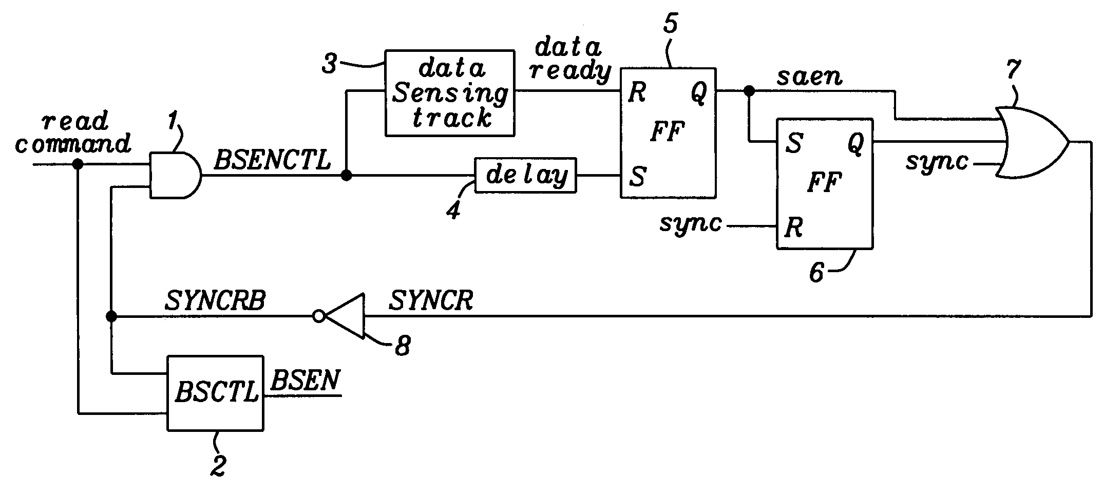
[0025]FIG. 1 shows a schematic block diagram of a circuit to reduce DRAM power consumption during a read-operation by reducing pre-charging of the bit-lines to a minimum and FIG. 2 shows time diagrams of the relevant signals issued by components of the circuit shown in FIG. 1.
[0026]An AND-gate 1 has a “read-command” and a “syncrb” signal as input; both signals are shown in FIG. 2. A bit switch control enablement signal “BSENCTL”, also shown in FIG. 2, is the output of this AND-gate 1. This enablement signal “BSENCTL” is the input for a circuitry 3 tracking the data sensing during a READ operation of a DRAM and for a delay circuitry 4. The delay circuitry 4 simulates the delay time of bit switch control unit BSCTL 2 generating BSEN signal. The bsoff t...
PUM
 Abstract
Description
Claims
Application Information