Method of forming contact hole and method of manufacturing semiconductor device

a technology of contact hole and manufacturing method, which is applied in the direction of semiconductor/solid-state device details, instruments, photomechanical equipment, etc., can solve the problems of difficult to obtain contact hole patterns at an equal size in the dense part and the less-dense part, and the difficulty of using these processes for the hole formation method, so as to reduce the opening size and reduce the opening size

Inactive Publication Date: 2008-04-22
KK TOSHIBA
View PDF7 Cites 18 Cited by
  • Summary
  • Abstract
  • Description
  • Claims
  • Application Information

AI Technical Summary

Benefits of technology

[0015]A method of forming a contact hole according to an embodiment of the present invention comprises exposing a resist film formed on a semiconductor substrate to a light using a first photomask in which mask patterns are arranged two-dimensionally at a predetermined pitch; developing the resist film to form contact hole patterns corresponding to the mask patterns in the resist film; reducing an opening size of each of the contact hole patterns formed in the resist film; exposing the resist film to the light using a second photomask in which predetermined patterns are formed to set a reflow starting temperature of a first resist film area that corresponds to the predetermined patterns to be relatively higher than a reflow starting temperature of a second resist film area other than the first resist film area; and heating the semiconductor substrate at a temperature equal to or higher than the reflow starting temperature of the second resist film area and lower than the reflow starting temperature of the first resist film area to subject the second resist film area to reflow and eliminate the contact hole patterns formed in the second resist film area.
[0016]A method of manufacturing a semiconductor device according to an embodiment of the present invention comprises forming a resist film on a semiconductor substrate; exposing the resist film to a light using a first photomask in which mask patterns are arranged two-dimensionally at a predetermined pitch; developing the resist film to form contact hole patterns corresponding to the mask patterns in the resist film; reducing an opening size of each of the contact hole patterns formed in the resist film; exposing the resist film to the light using a second photomask in which predetermined patterns are formed to set a reflow starting temperature of a first resist film area that corresponds to the predetermined patterns to be relatively higher than a reflow starting temperature of a second resist film area other than the first resist film area; heating the semiconductor substrate at a temperature equal to or higher than the reflow starting temperature of the second resist film area and lower than the reflow starting temperature of the first resist film area to subject the second resist film area to reflow and eliminate the contact hole patterns formed in the second resist film area; and etching the semiconductor substrate using the first resist film area to form contact holes in the semiconductor substrate.

Problems solved by technology

If contact hole patterns are to be formed on a resist film using such a photomask, it is conventionally, disadvantageously difficult to obtain contact hole patterns at an equal size in the dense part and the less-dense part.
In practice, therefore, it is difficult to use these processes for the hole formation method.
Namely, neither the RELACS® process nor the SAFIER® process can solve the disadvantage that the focus margin differs between the dense part and the less-dense part of the photomask.
Nevertheless, the reflow process is confronted with a disadvantage that the variation of the hole diameter is greatly influenced by accuracy of a heat process in the less-dense in comparison with the dense part.
It is disadvantageously necessary, therefore, to correct the photomask according to the opening pattern density.

Method used


Image

  • Method of forming contact hole and method of manufacturing semiconductor device
  • Method of forming contact hole and method of manufacturing semiconductor device
  • Method of forming contact hole and method of manufacturing semiconductor device

Examples


Embodiment Construction

[0025]An embodiment of the present invention will be described hereinafter with reference to the accompanying drawings.

[0026]FIGS. 5A and 5B are plan views of two photomasks X and Y used in the embodiment of the present invention, respectively.

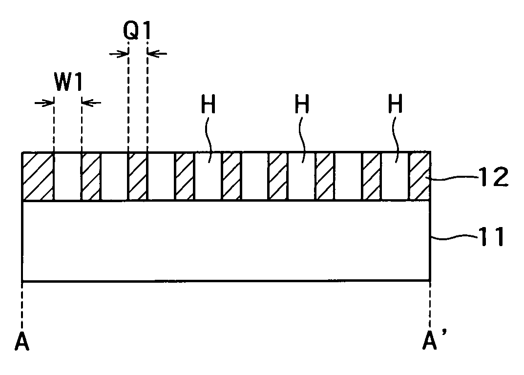
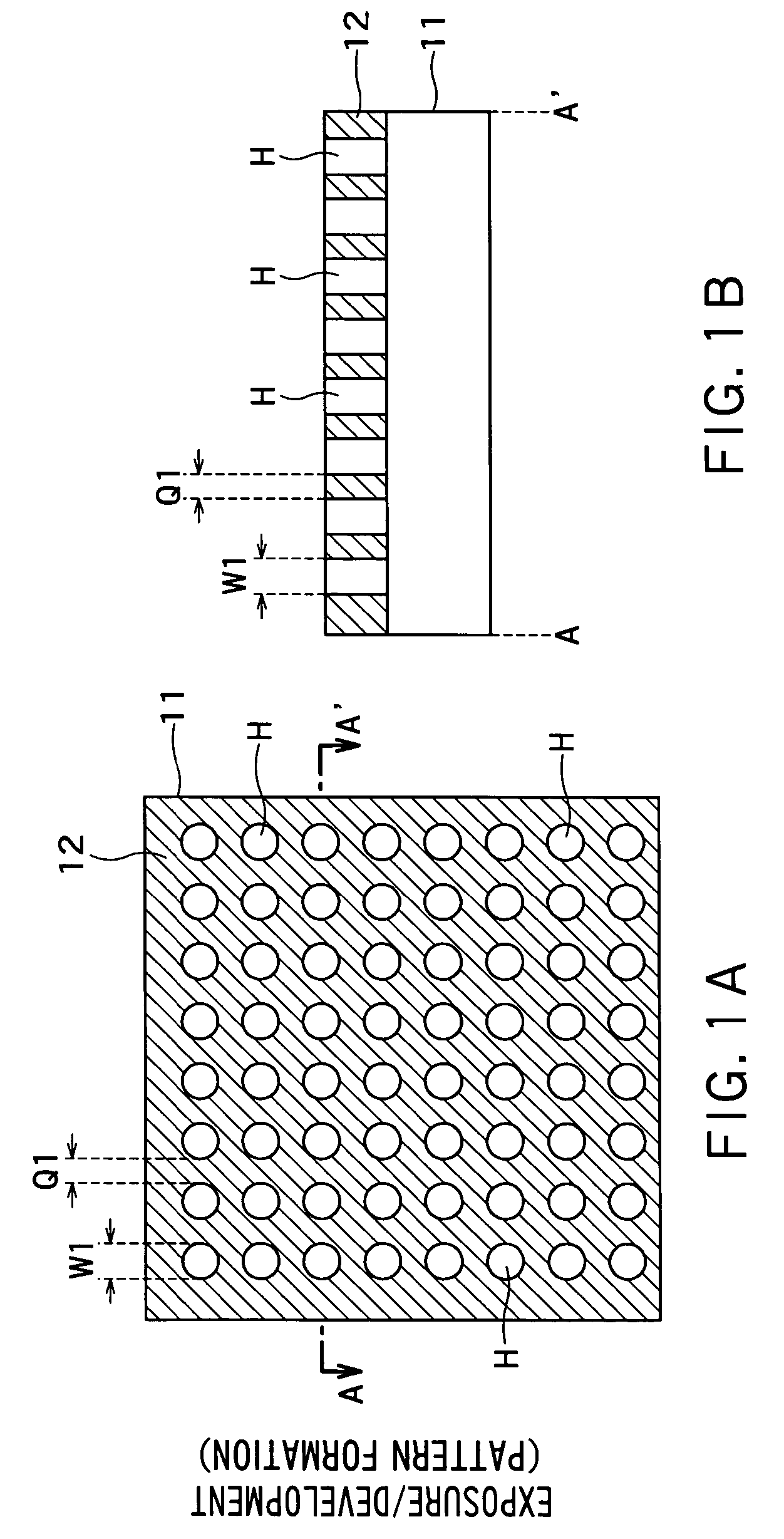
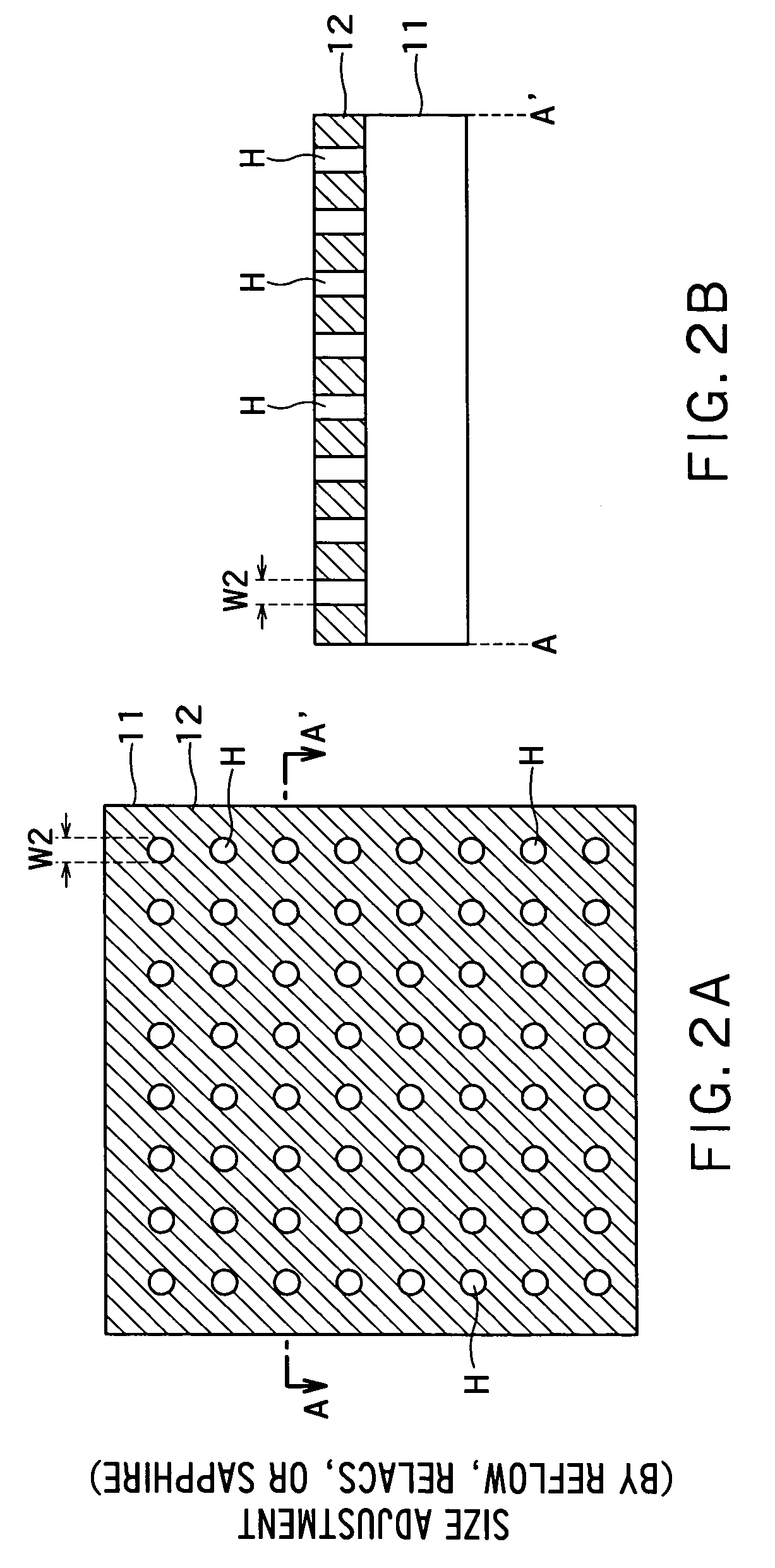
[0027]As shown in FIG. 5A, the photomask X is constituted so that mask patterns 2 each in a plane circular shape having a diameter of L1 are arranged at a pitch (an interval) P1 in a lattice fashion. The diameter L1 is, for example, 200 nm, and the pitch P1 is, for example, 300 nm. In FIG. 5A, parts surrounded by dotted lines 1a to 1c indicate mask patterns corresponding to finally formed contact holes, respectively, whereas remaining parts indicate dummy mask patterns. Specifically, the part surrounded by the dotted line 1a indicates the mask patterns arranged at high density, and the parts surrounded by the dotted lines 1b and 1c indicate the mask patterns arranged at low density, respectively.

[0028]As shown in FIG. 5B, the photomask Y inclu...


PUM

PropertyMeasurementUnit
diameter L1aaaaaaaaaa
thicknessaaaaaaaaaa

Abstract

A method of forming a contact hole according to an embodiment of the present invention comprises exposing a resist film formed on a semiconductor substrate to a light using a first photomask in which mask patterns are arranged two-dimensionally at a predetermined pitch; developing the resist film to form contact hole patterns corresponding to the mask patterns in the resist film; reducing an opening size of each of the contact hole patterns formed in the resist film; exposing the resist film to the light using a second photomask in which predetermined patterns are formed to set a reflow starting temperature of a first resist film area that corresponds to the predetermined patterns to be relatively higher than a reflow starting temperature of a second resist film area other than the first resist film area; and heating the semiconductor substrate at a temperature equal to or higher than the reflow starting temperature of the second resist film area and lower than the reflow starting temperature of the first resist film area to subject the second resist film area to reflow and eliminate the contact hole patterns formed in the second resist film area.

Description

CROSS-REFERENCE TO RELATED APPLICATIONS[0001]This application claims the benefit of priority under 35USC §119 to Japanese Patent Application No. 2003-355084 filed on Oct. 15, 2003, the entire contents of which are incorporated herein by reference.BACKGROUND OF THE INVENTION[0002]1. Field of the Invention[0003]The present invention relates to a method of forming a contact hole and a method of manufacturing a semiconductor device. More specifically, the present invention relates to a method of forming a contact hole and a method of manufacturing a semiconductor device each including a step of adjusting an opening size of contact hole patterns formed in a resist film.[0004]2. Related Background Art[0005]In recent manufacturing of a semiconductor device a scale-down of which is advanced, not only a wavelength of an exposure light used to form a resist pattern at a lithography step is made shorter, but also a certain processing is additionally performed after forming the resist pattern, ...

Claims


Application Information

Patent Timeline
Patent Type & Authority Patents(United States)
IPC IPC(8): G03F7/00G03F1/00G03F1/68G03F7/20G03F7/40H01L21/027H01L21/28H01L21/30H01L21/3205H01L21/44H01L21/768H01L23/52H01L23/522
CPCH01L21/76816G03F7/40H01L21/0274G03F1/70
Inventor KOBAYASHI, YUJI
Owner KK TOSHIBA
Why Eureka
Try Eureka