Semiconductor apparatus and method of manufacturing the same

a technology of semiconductor devices and semiconductors, applied in the direction of semiconductor devices, electrical devices, transistors, etc., can solve the problems of parasitic bipolar transistors to turn, device breakdown, device breakage, etc., and achieve the effect of reducing cell size and preventing the reduction of device breakdown toleran

Active Publication Date: 2008-04-22
RENESAS ELECTRONICS CORP
View PDF9 Cites 147 Cited by
  • Summary
  • Abstract
  • Description
  • Claims
  • Application Information

AI Technical Summary

Benefits of technology

[0018]According to an embodiment of the invention, there is provided a semiconductor apparatus that includes a semiconductor substrate of a first conductivity type, a base region of a second conductivity type formed on a principal surface of the semiconductor substrate, a trench has a substantially octagonal plane shape and formed in a periphery of the base region, and an endless source region of the first conductivity type formed on a surface of the base region along the trench. In this semiconductor apparatus, the principal planes on side surfaces of the trench are composed of planes [100] and [110]. A minimum distance between the base region and the plane [110] facing each other through the source region is shorter than a minimum distance between the base region and the plane [100] facing each other through the source region.
[0019]With this configuration, the present invention can prevent a decrease in device breakdown tolerance while achieving reduction of cell size. This is because of the following reasons.
[0020]Since the present invention forms the principal plane directions of the trench side surfaces with [100] and [110] and the trench has a substantially octagonal plane shape, it is possible to ease the concentration of current at a channel along a cell corner compared with a rectangular cell.
[0021]Further, since the minimum distance between the base region and the trench side surface composed of the plane [110] that face each other through the source region is shorter than the minimum distance between the base region and the trench side surface composed of the plane [100] that face each other through the source region, it is possible to reduce the distance that current passes through the base region as a whole in a unit cell compared with the case where the trench side surface is composed of only the plane [100] even when part of dielectric current flows into the base. This allows suppression of an increase in base voltage even if part of dielectric current flows into the base. As a result, this structure hinders the activation of a parasitic bipolar transistor, thus preventing a decrease in device breakdown tolerance.
[0022]Furthermore, since the trench of this embodiment has a simple structure where the principal plane direction of the trench side surface is formed with [100] and [110], and the trench has a substantially octagonal plane shape, it is possible to achieve reduction in cell size.
[0023]As described above, the present invention has a beneficial effect that provides a semiconductor apparatus capable of preventing a decrease in device breakdown tolerance and achieving reduction in cell size.

Problems solved by technology

Since the vertical power MOSFET is used in connection with an inductor, reverse withstand voltage is applied between the drain and source during switch-off, and current flow beyond a certain design limit can result in breakdown of devices.
Specifically, if part of dielectric current flows into the base as shown by a current path d that is indicated by the arrow in FIG. 9B and a base voltage increases, the parasitic bipolar transistor turns on to apply positive feedback during a temperature increase and a current increase, which eventually causes device breakdown.
Breakdown thereby tends to occur at the cell corner and its vicinity, which can cause the parasitic bipolar transistor to turn on.
However, the semiconductor apparatus according to Japanese Unexamined Patent Publication No. 2001-60688 is unfavorable for the further reduction of cell size since it needs to place the narrow source region 116.
The semiconductor apparatus according to Japanese Unexamined Patent Publication No. 09-213951 is also unfavorable for the further reduction of cell size since the trench is composed of a combination of octagon and quadrangle shapes.

Method used


Image

  • Semiconductor apparatus and method of manufacturing the same
  • Semiconductor apparatus and method of manufacturing the same
  • Semiconductor apparatus and method of manufacturing the same

Examples


embodiment 1

Alternative Embodiment 1

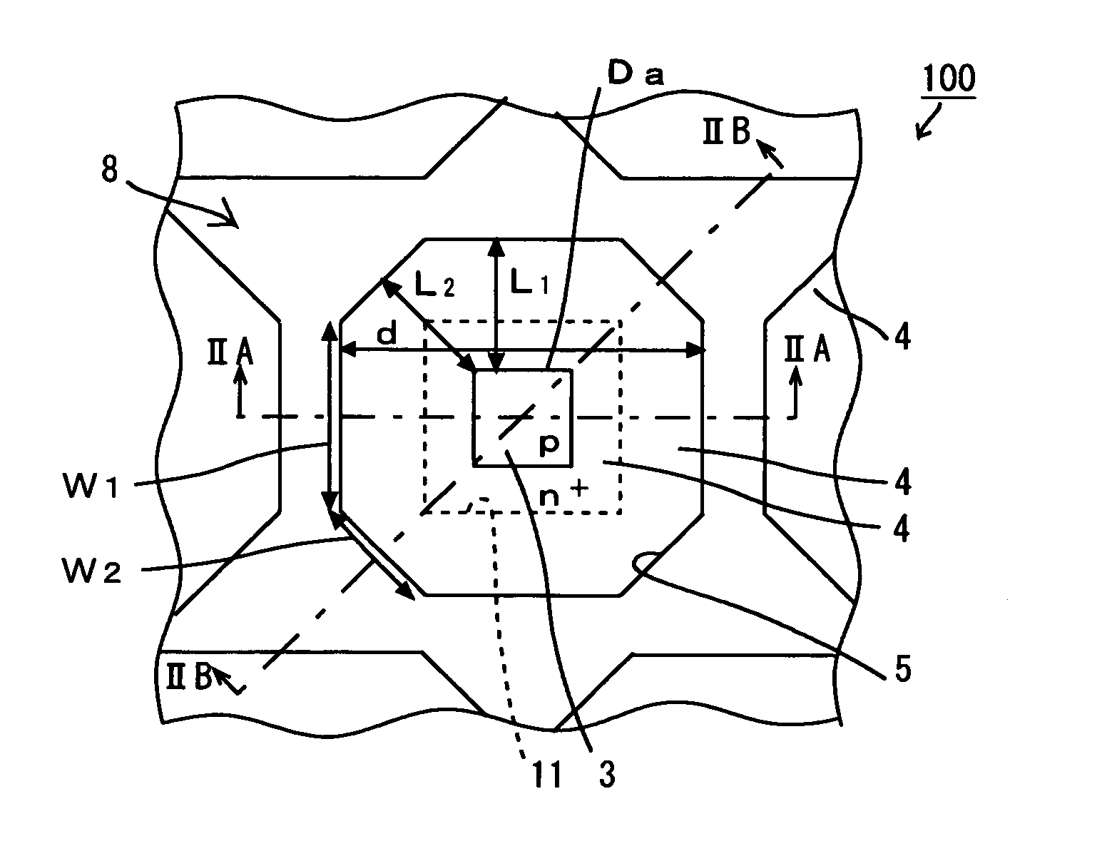
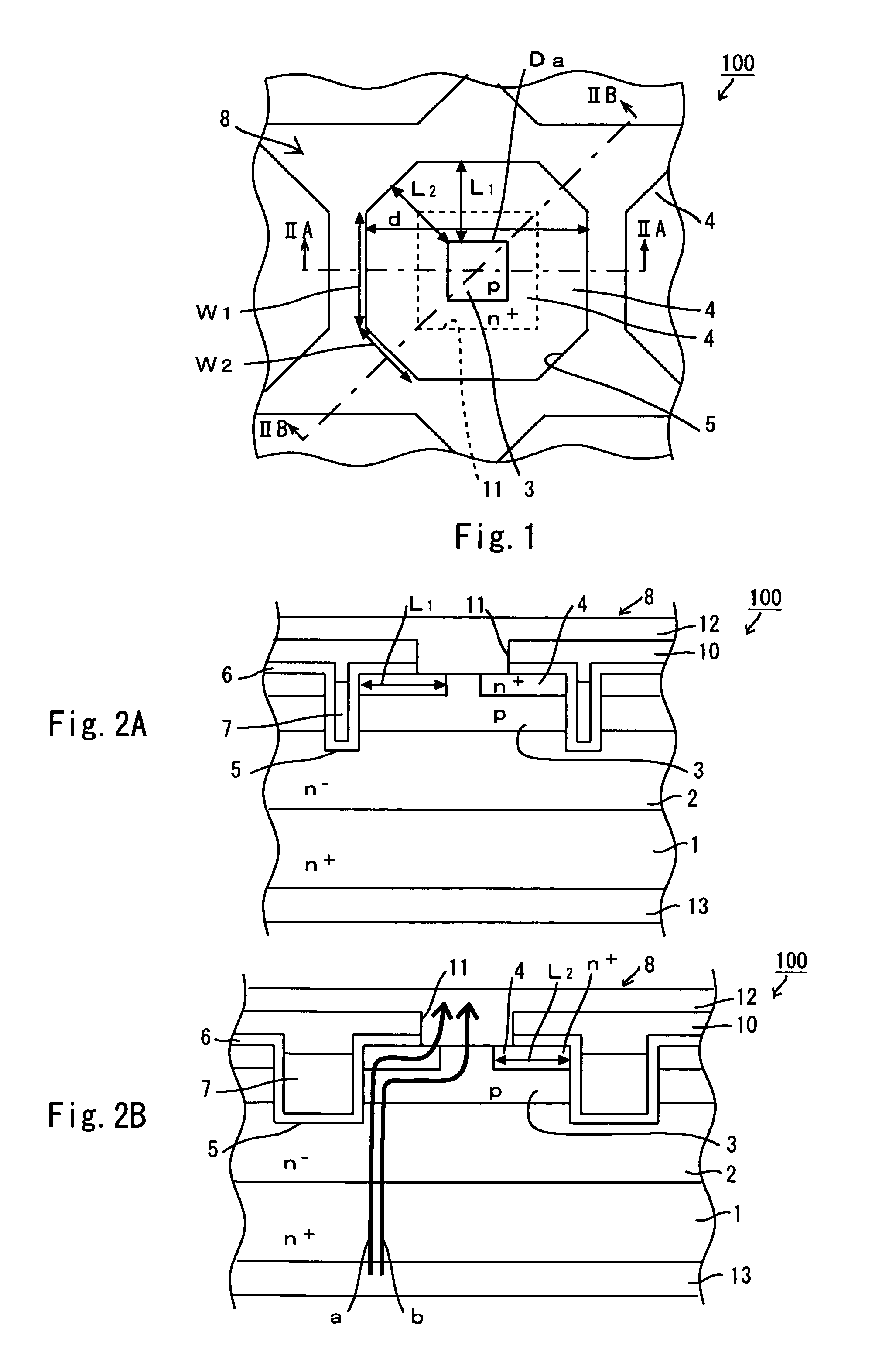
[0079]An alternative embodiment having a trench structure that is different from the above embodiment is described hereinafter. FIG. 6 is a plan view showing the trench structure of the alternative embodiment 1. In the following description, the same elements as in the above embodiment are denoted by the same reference symbols and not detailed herein.

[0080]The semiconductor apparatus 200 of the alternative embodiment 1 has basically the same structure as the above embodiment except for the following points. Though the trench 5 of the above embodiment is an octagon having W1 and W2, a trench 5a of this alternative embodiment is an octagon having W1, W2 and W3 as shown in FIG. 6. Further, though the base region 3 of the above embodiment has a substantially square plane shape, a base region 3a of this alternative embodiment has a substantially rectangle plane shape.

[0081]Specifically, the sides of the plane [100] on the side surface of the trench 5a are indicate...

embodiment 2

Alternative Embodiment 2

[0084]An alternative embodiment having a trench structure that is different from the above embodiment is described hereinafter. FIG. 7 is a plan view showing the trench structure of the alternative embodiment 2.

[0085]The semiconductor apparatus 300 of the alternative embodiment 2 has basically the same structure as the above embodiment except for the following points. Though the internal angle of adjacent side surfaces of the base region 3 is 90° in the above embodiment, a corner between adjacent side surfaces of the base region 3b is rounded in this embodiment as shown in FIG. 7. In other words, the source region 4 includes an electrode connecting area that connects a source electrode. The electrode connecting area has four sides that are parallel with the plane [100] and corners that are rounded.

[0086]This structure allows easing the concentration of base current density at a base corner part. It is therefore possible to suppress a base voltage drop more ef...


PUM


Abstract

A semiconductor apparatus includes a semiconductor substrate of a first conductivity type, a base region of a second conductivity type formed on a principal surface of the semiconductor substrate, a trench formed in a periphery of the base region, and an endless source region of the first conductivity type formed on a surface of the base region along the trench. In this semiconductor apparatus, the principal planes on side surfaces of the trench are composed of planes [100] and [110]. The interior angle of intersection of adjacent side surfaces of the trench is 135°. A minimum distance between the base region and the plane [110] facing each other through the source region is shorter than a minimum distance between the base region and the plane [100] facing each other through the source region.

Description

BACKGROUND OF THE INVENTION[0001]1. Field of the Invention[0002]The present invention is related to a semiconductor apparatus having a trench structure and a method of manufacturing the same.[0003]2. Description of Related Art[0004]A power metal-oxide semiconductor field-effect transistor (MOSFET) is a typical semiconductor apparatus that has both a high withstand voltage and a large current capacity. There are two types of power MOSFET: lateral power MOSFET and vertical power MOSFET. The lateral power MOSFET is designed so that operating current (drain current) flows horizontally through a semiconductor substrate. The vertical power MOSFET is designed so that drain current flows vertically through a semiconductor substrate. The vertical power MOSFET has become common since it is superior to the lateral power MOSFET in being easy to realize a high density unit cell structure and thus allowing an increase in on-current. Particularly distinguished is a vertical power MOSFET having a t...

Claims


Application Information

Patent Timeline
Patent Type & Authority Patents(United States)
IPC IPC(8): H01L29/76
CPCH01L29/4236H01L29/66734H01L29/7813H01L29/045H01L29/0696H01L29/4238H01L29/7811
Inventor MIURA, YOSHINAOOHTANI, KINYA
Owner RENESAS ELECTRONICS CORP
Why Eureka
Try Eureka